J5 pins 13, 15, 17 and 19:
src4392cclk -> U9 pin 20
src4392csn -> U9 pin 19
src4392cdin -> U9 pin 21
srcdixrstn -> U9 pin 24 and U8 pin 24
Is there some big solder bridge at U9? Did you really measure a resistance < 10 ohm?
J5 pins 57, 75 and 67:
bckout, U9 pin 48
dix4192cdout, U8 pin 22
lrck, U8 pin 38
This doesn't make sense even with a solder bridge.
When the test voltage of your meter is greater than a volt or so, you will always measure some slightly conducting path between any pair of pins of U8 and U9 due to their ESD protection diodes. If you measure only a few ohms or even less, there is really something wrong.
Last edited:
Have not been checking for adjacent pin shorts specifically, but have been making sure the correct FPGA pin has contact to the right 'other' pin.
Could the problem be something to do with the switches? I am not populating the 'Surprise' mode.
SW5 is not populated (left open)
SW4 is not populated and is shorted to 'loud'
SW3 has four positions one of which is engaged but I am still using the P9 I2S input which should override this (no 5 position switch here yet). Tried quite early in the process to unplug SW3 but have not done it lately, perhaps I should.
SW2 has three positions with 'surprise' not connected to the switch
SW1 has three positions with 'surprise' not connected to the switch
I think that is all just fine, but you can do the SW3 check just in case I'm mistaken.
When you checked the presence of 3.3 V at open switch contacts, did you also check SW5 and the surprise positions of SW1 and SW2?
J5 pins 13, 15, 17 and 19:
src4392cclk -> U9 pin 20
src4392csn -> U9 pin 19
src4392cdin -> U9 pin 21
srcdixrstn -> U9 pin 24 and U8 pin 24
Is there some big solder bridge at U9? Did you really measure a resistance < 10 ohm?
J5 pins 57, 75 and 67:
bckout, U9 pin 48
dix4192cdout, U8 pin 22
lrck, U8 pin 38
This doesn't make sense even with a solder bridge.
When the test voltage of your meter is greater than a volt or so, you will always measure some slightly conducting path between any pair of pins of U8 and U9 due to their ESD protection diodes. If you measure only a few ohms or even less, there is really something wrong.
Am not actually looking at the measured resistance rather letting the beep tell me there is continuity. Looking at the DMM manual the beep threshold is < 8% for up to 500R, so less than 40R resistance to make a beep...I think. If the beep was sketchy I would look at the resistance reading which generally improved with more careful probe placement.
I'll check these things more carefully tonight. Thanks so much for your help.
Another possibility is that there could be something wrong with the 27 MHz clock after all:
A. Duty cycle and constraints
The user constraints file I used when implementing the design specifies a 50 % duty cycle for the 27 MHz clock, but in reality the duty cycle is larger (due to a 5 V clock signal with relatively weak slopes getting level translated to 3.3 V). It could be that due to this, the timing is not clean and Sonny and I are just lucky that our valve DACs work. I must have been lucky several times then, as I've had three different FPGA boards in mine and it always worked, also with several different versions of the configuration file, but still.
I'll describe a possible experiment after having breakfast.
B. Clock spikes that are too narrow to see on your scope, but still trigger the FPGA
If the FPGA is clocked twice in every clock cycle, then it will detect that the clock frequency is way out of range and refuse to continue with its start-up procedure. I can think of two things that could cause this:
B.1. Wrong transmission line termination
R124 is 33 ohm, as intended, but that 33 ohm is based on a 360 um prepreg layer thickness. Do your boards have 360 um thick prepreg?
B.2. Self-oscillations of U17E
Is U17 an SN74AHCU04 (correct) or an SN74AHC04 (incorrect)?
Does connecting a 2.2 pF capacitor in parallel with C17 change anything?
Am not actually looking at the measured resistance rather letting the beep tell me there is continuity. Looking at the DMM manual the beep threshold is < 8% for up to 500R, so less than 40R resistance to make a beep...I think.
Sounds like there must be something wrong, as I can't imagine you get such a low reading due to the ESD diodes.
If it is still relevant after debugging this weird continuity test result, you could try this to trim the clock duty cycle:
-Connect a 10 kohm resistor to the node C13-R51, and keep the wire from this node to the resistor body short.
-Connect the other side of the 10 kohm resistor to the wiper of a potmeter, the wire length on this side shouldn't be critical. Connect the other terminals of the potmeter to +5 V and ground with whatever wire length you need.
-Measure the signal between R124 and ground with your oscilloscope and 1:10 probe and trim the potmeter until the signal looks as symmetrical as possible
-Disconnect the probe and see if the relays work now
Last edited:
There is another clock here still sitting on the pcb I damaged earlier. May be able to swap that one in but did not bother desoldering it because I was a little worried about damage of a $2 item. But it is a possibility.
The pcbs have been built to the exact specifications early in this thread. I actually called the fab house to make sure they were picking up what you were putting down and was assured all was in order. Not sure how I would be able to check it though.
Looks like the correct U17. This is the exact one I ordered...
SN74AHCU04D Texas Instruments | Mouser Australia
Will have a look later for a 2.2pF cap. First thing to do is to verify my continuity observations.
The continuity tests were a shambles.
J5.13/15/17/19 all have <0.3R resistances to their pairs on U9.
But J5.13 also makes the following connections:
-> U9.24 <0.3R
-> U9.23 no connection
-> U9.22 no connection
-> U9.21 no connection
-> U9.20 <0.3R
-> U9.19 <0.3R
-> U9.18 <0.3R
-> U9.17 175R
-> U9.16 <0.3R
-> U9.15 500R
-> U9.14 450R
-> U9.13 <0.3R
Yes, a couple of those are to ground.
So I went around measuring resistances across capacitors and they basically fell into four groups:
175R across them: C80, 93,35
260R across them: C66
425R across them: C43, 82, 93, 87, 117, 116
545R across them: C115, 81, 68, 125
High resistance: C72, 71, 76, 70, 75, 69, 74, 77, 85, 108, 97, 95, 89, 86, 121, 123, 167, 130, 124, 94, 86, 127
Did not measure all of the caps. Got to the first caps in the reconstruction filter. Three of them measured high resistance but one of them (C51) measures 7.5R. The corresponding output cap C54 also measures 7.5R Looks like the problem is somewhere there. RV1 and RV2 both seems to measure sensible resistance between the three pins but the R76/103/104 string measures much less than the other three anode resistor strings.
Marcel, would a problem in this area correlate to a digital issue at the FPGA and those crazy continuities listed at the head of this post? I'm going to have dinner and if I get some time will desolder some of the anode resisitors and caps to see how they measure out of the circuit.
It sounds to me like you have at least three shorts to ground in the digital part, one on the src4392cclk line (supposed to be connected to J5.13 and U9.20), one on the srcdixrstn line (supposed to be connected to J5.19, U8 pin 24 and U9 pin 24) and one on src4392csn (J5.15 and U9 pin 19). Please don't power up the circuit with the FPGA module installed until those are solved, as shorting a digital output could blow up the FPGA's I/O cell.
I wouldn't be too worried about the hundreds of ohms readings for the time being. There is probably some path through ESD protection diodes and/or switched off supplies that causes those.
It also seems like there is a short from C51/C54 to ground. That's not good, but at least it can't cause any damage.
It sounds to me like you have at least three shorts to ground in the digital part, one on the src4392cclk line (supposed to be connected to J5.13 and U9.20), one on the srcdixrstn line (supposed to be connected to J5.19, U8 pin 24 and U9 pin 24) and one on src4392csn (J5.15 and U9 pin 19). Please don't power up the circuit with the FPGA module installed until those are solved, as shorting a digital output could blow up the FPGA's I/O cell.
I don't know how I am going to find these shorts. All pin and pad contacts look clean under the magnifying glass. Perhaps I should start desoldering things until the shorts are revealed.
I wouldn't be too worried about the hundreds of ohms readings for the time being. There is probably some path through ESD protection diodes and/or switched off supplies that causes those.
That is also what I thought. Hoped it may help to diagnose just where the problem lies.
It also seems like there is a short from C51/C54 to ground. That's not good, but at least it can't cause any damage.
C51 was gone. Pulled it out of the circuit and it is shorted (7.5R). Quite sure it was ok going in because I normally run those important caps over the LCR meter to make sure they match the filter values.
If you can't find anything related to soldering that explains those shorts, do you also have shorts to ground on the unpopulated spare boards? Maybe something went wrong during processing due to the non-standard stack-up.
This occured to me over dinner last night. In the end I did not want to know for sure in case I lost sleep, but this morning refreshed I was unable to replicate the shorts on a bare board.
I don't know how I am going to find these shorts. All pin and pad contacts look clean under the magnifying glass. Perhaps I should start desoldering things until the shorts are revealed.
Desoldering SMD ICs is not easy unless you have a hot air station, although some forum members know tricks to do it without.
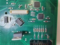
All nets that are shorted to ground are on the same side of U9, U9 pins 19, 20 and 24, while pin 18 is a ground pin. Does resoldering that side of U9 improve anything?
Had a 'moment' earlier when considering options for debugging these shorts. Would really hate to damage the pcb again in my haste and needed low-risk methods to not lose what I already have. At the time I was thinking that perhaps I buy some more bits and slowly build up the digital section on a new pcb to see where the problem occurs and then see if I can remedy the fully built up pcb. Then it occured to me that I already have a built up pcb...the one I ruined with the standoff/FPGA/impatience some time ago...so I went and checked and it seems like I have all the same shorts on that pcb as I have on this new one.
Don't know whether that is good or bad but it does mean that I have a dead board to practice on. It also means that either I have made the same mistake/s twice or that the pcb is dysfunctional (hopefully the former). Could it be as simple as incorrect orientation in the Ux sockets? This has been checked but perhaps I got it wrong both times..
Don't know whether that is good or bad but it does mean that I have a dead board to practice on. It also means that either I have made the same mistake/s twice or that the pcb is dysfunctional (hopefully the former). Could it be as simple as incorrect orientation in the Ux sockets? This has been checked but perhaps I got it wrong both times..
- Home
- Source & Line
- Digital Line Level
- Valve DAC from Linear Audio volume 13