Not exactly. let's open the schematic in a separate window and take a look at it
https://puredsd.ru/BBBreclk.pdf
it has stuffs on it. The top two rows with U2 and U3 are the clocks. U7 is a selector that sends one of two clock signals, depending on CLK_select2. The next rows with U4 is a 3.3v power supply feeding the stuffs below it.
U1 is a multiplexer IC. Think of it as a computer router. If the DSD_on pin is selected, it sends DSD data to BCK1, LRCK1, and Data1. If it is not, it sends PCM data to these pins.
U5 and U6 are the isolators. This is Hermes. Just 2 ICs. Now, Zoran pointed out the design flaw here
"The goal is to keep separate I2S lines all of the transition lines.
Not to merge all I2S lines into single IC. and multiple times.
The lines are from different frequency and for my opp should not be interfered in the small space die-s in ICs...
I have good results with single digital isolator ADuM1100"
https://www.diyaudio.com/forums/digital-line-level/358147-simple-dsd-src-beaglebone.html#post6296233
His suggestion is to use a separate isolator for each line.
U8, U9, and U10 are the reclocker. Just 3 flip flops. See the link to the article that I posted earlier. This is Cronus. Just 3 ICs, plus circuit to connect the clocks.
So, when I asked whether we need reclocker, I am asking whether these 3 flip-flops are necessarily. The answer seems to be no.
In fact a super duper Zoran-inspired BBB-Valve Dac (DSD only) cape can be made with U7 connected to two external very good clocks, one 2-pin connector to accept an external power supply, and separate digital isolator for each line (more of those U5 and U6 ICs). U1 and U8 are gone. Not sure what connectors people like. I guess u.fl for the high speed data lines and just a regular 3-pin for the low speed mute, dsd_on lines.
Last edited:
I surely will use those u.fl pads. BBB is great for audio because that pin 25 MCK-in. We can feed a clock back to the BBB. I think, but am not 100% sure, that a PI does not accept external clock. So, reclocking is necessarily in a Pi, in a dac using usb or s/pdif input. BBB here, I think not.
Last edited:
Raja, your PM box seems to be full!
Ray
Sorry, Ray. Please try again.
pgour -1xPCB + 2x filter PCB (GREECE)diyAchim - 1 x PCB - 1 x SMD Parts installed - 1 x Filter PCB (pair) - Country = Germany
Raj!1 - 1 PCB - 1 x SMD parts installed - country = UK
dubulup - 2 x PCB - 0 x SMD Parts installed - 2 x Filter PCB (pair) - Country = USA
ericoto -1 PCB
HenSch - 2x PCB, 2x Filter PCB (pair) country=Germany
mterbekke - 2 times everything (2pcb+soldering+filter (Netherlands, confirmed)
rfbrw - 1 PCB Filter PCB 1 set.(UK)
Pistollero - 1 PCB (Portugal)
luchoh - 1 PCB + 1 SMD Parts installed + 2 Filter PCB (USA)
agent.5 - 1 PCB + 1 SMD Parts installed + 2 Filter PCB -> USA
spm - 1 PCB, no SMD, 4 x filter PCB (UK)
torb - 1 PCB + 0 SMD Parts installed + 0 Filter PCB (Finland)
thuanth43 - 1 PCB + 0 SMD parts installed (Singapore)
Kcom00 - 1 x PCB + 2 x Filter PCB (Australia)
Not exactly. let's open the schematic in a separate window and take a look at it
https://puredsd.ru/BBBreclk.pdf
it has stuffs on it. The top two rows with U2 and U3 are the clocks. U7 is a selector that sends one of two clock signals, depending on CLK_select2. The next rows with U4 is a 3.3v power supply feeding the stuffs below it.
U1 is a multiplexer IC. Think of it as a computer router. If the DSD_on pin is selected, it sends DSD data to BCK1, LRCK1, and Data1. If it is not, it sends PCM data to these pins.
U5 and U6 are the isolators. This is Hermes. Just 2 ICs. Now, Zoran pointed out the design flaw here
"The goal is to keep separate I2S lines all of the transition lines.
Not to merge all I2S lines into single IC. and multiple times.
The lines are from different frequency and for my opp should not be interfered in the small space die-s in ICs...
I have good results with single digital isolator ADuM1100"
I don't see why that would make any difference when those signals are synchronized with a clean clock anyway by U8, U9 and U10. I do understand that U8 has to be kept separate from U9 and U10 to prevent crosstalk from data to clock, but that's indeed done.
By the way, it would have been better to ground the I0a and I1a inputs of U1. You now get overlap currents that depend on what random voltage those floating inputs float to.
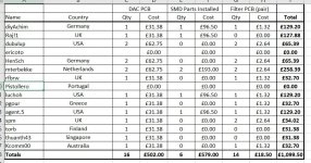
GB Now Closed
The Group Buy is now closed for subscriptions!
I will be looking to get the PCBs ordered by next weekend and will advise you of the final cost of the PCB's you've requested soon. I will order 15 main PCBs (I already have one spare from the original board purchase to make the 16) and 30 filter PCBs.
Once I have the PCBs ordered I will move onto the smd parts and soldering as a separate exercise.
As I already have one PCB available one lucky person will get there PCB shipped this week. That will be torb in Finland who is the first subscriber only requiring a main board.
Below is where we are with choices - I'm still waiting on input from ericoto and Pistollero.
Attachments
Last edited:

I don't see why that would make any difference when those signals are synchronized with a clean clock anyway by U8, U9 and U10. I do understand that U8 has to be kept separate from U9 and U10 to prevent crosstalk from data to clock, but that's indeed done.
By the way, it would have been better to ground the I0a and I1a inputs of U1. You now get overlap currents that depend on what random voltage those floating inputs float to.
I don't know much about digital isolators. There is probably a difference in the GHz or above. Under 50MHz, maybe there is a difference under a full moon in a warm summer night, or not.
The cost is $1.89 for a single channel and $4.40 for three channels. TL1431 is like $0.26 each.
https://www.mouser.com/ProductDetail/Analog-Devices/ADUM110N1BRZ?qs=pyvxRoUzNN97PahA7Gg2Jw==
ADUM1301ARWZ-RL Analog Devices | Mouser
Multi-channel is slightly cheaper per channel. It makes a huge difference to OEMs counting pennies. But for DIYers making just 1 or 2, it probably makes no difference, and may as well go all mono.
Marcel, I've attached a zip file with mechanical drawings of the PCB if you wouldn't mind adding them to the first post.
I produced the drawing in Front Panel Designer (FPD), the software used by Schaeffer and Front Panel Express, which is easy to use and free to download. I've included the FPD file and also an export to dxf for those who want a CAD drawing. If you just want to print a drilling template you can export from FPD to pdf to print out (scaling set to 100% of course).
The drawing includes the outline, stand-off holes, valve socket locations andthe pin1 location of the input and output headers (input header pin location was important for me to correctly position the BBB and reclocker).
I obtained the XY coordinates of the mounting holes etc. by opening the PCB gerber files in a free online gerber viewer.
Reference Gerber Viewer, by the developer of the Gerber Format
Attachments
Marcel, I've attached a zip file with mechanical drawings of the PCB if you wouldn't mind adding them to the first post.
I can't attach anything to the first post, but I've added a link to post #751.
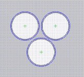
Regarding the mechanical drawings, I know some are thinking about having the valves projecting through the top of the chassis as I have done with my build. You might want to be aware that the trios of valves don't form symmetrical triangles -the 'lower' valve is offset from the centreline between the upper valves by about 1mm. I've attached a screengrab of part of my chassis top plate drawing to, hopefully, illustrate what I mean.
Ray
Ray
Attachments
diyAchim - 1 x PCB - ? x SMD Parts installed - ? x Filter PCB (pair) - Country = ?
Raj!1 - 1 PCB - 1 x SMD parts installed - country = UK
dubulup - 2 x PCB - 0 x SMD Parts installed - 2 x Filter PCB (pair) - Country = USA
ericoto -1 PCB, 1 SMD parts installed, filter PCB
HenSch - 2x PCB, 2x Filter PCB (pair) country=Germany
mterbekke - 2 times everything (2pcb+soldering+filter (Netherlands, confirmed)
rfbrw - 1 PCB Filter PCB 1 set.(UK)
Pistollero - 1 PCB (Portugal)
luchoh - 1 PCB (USA)
pgour - 1 PCB
agent.5 - 1 PCB + 1 SMD Parts installed + 2 Filter PCB -> USA
spm - 1 PCB (UK)
torb - 1 PCB (Finland)
thuanth43 - 1 PCB (Singapore)

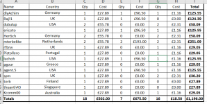
I got a very quick response from PCBway - at today's exchange rate the cost per main DAC PCB will be £26.50 (including shipping to me but excluding onward shipping). I will PM everyone later today with my PayPal account to start collecting deposits. I will order the PCBs once I have the deposits.
That cost is based on ordering 20 PCBs. That means we will have 2 spare PCBs so can I make a suggestion regarding them. As the full cost of the 20 PCBs will be covered by your payments, I will hold the spare PCBs and if someone requires one later I will sell at £26.50 and donate the proceeds to DIY Audio. Does anyone object to that?
I will get the cost for the Reconstruction Filter PCBs later this evening.
Ray
I have these transformers for many years... just wondering if it’s possible to use them as output transformers? They are 1:1 ratio with many taps 50/125/333/500.
I'm sure it is. With a circuit like in post #215, connect pins 3 and 4 to each other and to R2. Short pins 9 and 10. Connect L1-C2-R1 to pin 1, connect L4-C6-R4 to pin 6, connect pin 7 to R3 and connect pin 12 to C9.
The only thing is that the values of R3 and C9 are optimized for the Lundahl transformer, so you may have to tweak them to get the flattest possible response. If you could find a datasheet or application note for your transformer, it may already specify the optimal values.
- Home
- Source & Line
- Digital Line Level
- Valve DAC from Linear Audio volume 13