AIM65 please read the post #19, we have tried with reclock with the clock provided by ours i2s source, also.
Except you meant, that the pulse that introducing into the flip-flop chips not to be the external clocks but the same amanero's mclk.
In my setup, I can tried it easily.
Except you meant, that the pulse that introducing into the flip-flop chips not to be the external clocks but the same amanero's mclk.
In my setup, I can tried it easily.
I can try that, even though I've checked the MCLK both at its source (Si570) and on the 4490's pin and they look pretty much identical.
The 4490s appear to be pretty tolerant of the MCLK. I've tried MCLKs starting at ~11MHz (the lowest specified) with no change. Manolis even tried a 3MHz signal that he had available, and the 4490 still produced sound (even though it had a lot of THD..). Even with a completely wrong MCLK, the chip works, even though the THD increases to over 3%.
You mean to put a 50R resistor before each flip-flop, plus keep the R4 resistors, right?
Information on proper termination of signals of this kind is kindda sketchy.. I've done a lot of reading and I still haven't got a proper grasp on it.
In case of the resistors before the flip-flops, shouldn't the termination be of "parallel" type? Via resistors to gnd? But since the source of the I2S signal will be "seeing" two resistors in parallel, it will be seeing half the resistance. But an even better way to go about it would be to buffer & split the signals properly. But that adds jitter. And so on, and so forth..
So I just left the signal as it was, improperly terminated. The pulses look just fine on the ol' scope, so it should be working OK.
We've tried both with the Si570 and without, with MCLK coming either from Acko's reclocker or directly from the Amanero with the same results. What I haven't tried (and I believe neither has Manolis) is Acko's reclocker on a single-4490 board with no reclocking. But I might be mistaken.. He'll let us know.
See above, they are not, but that doesn't seem to impact the shape of the pulses.
I will try the inversion of the MCLK.
This is not a question a termination, termination issue is for the UFL links, and you right : termination resistors have to be connected to gnd.
The point here is about damping the LC networks formed, at MCLK frequency, by the input cap of the chip (CMOS one) and the pcb layout. This is why we add damping resistors in order to have an RLC with Q factor under control.
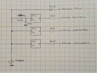
My idea was to remove R1 and to have one resistor in serial with MCLK of 4490A and one in serial with MCLK of 4490B (by the way could you post a larger part of the schematic in order to see all the connections of MCLK ?)
About the damping resistor of the 3 D latch : I wouldn't use them, but if you need them it should one in serial per D latch.
About your measurement with the scope : connecting the probe add few pF and may dramatically change the waveform, f0 and Q factor of the LC. The measurement process change the measured value...
Last thing, and I'm not sure this could be another error in AKM documents, on app notes of AK4490 and 4495 the damping resistor of MCLK is 5.1R, not 51R. 51R is for the slower signal : LRCK, BICK and SDATA
Last edited:
I am not sure how this is done in this context. But in synchronous digital circuits, the D input to a flipflop has to be synchronously generated to the clock on the CLK input of the flipflop. Otherwise, this will result in metastability and incorrect sampling.
The two clocks cant simply be of the same frequency, but to be synchronous they have to be from the same source.
Further their phases have to be such that the D input can meet flops setup/hold requirement with respect to the clock input.
Sorry if this doesnt apply in the context of reclocking the I2S stream, i have to read in more details to understand.
AIM65 please read the post #19, we have tried with reclock with the clock provided by ours i2s source, also.
Except you meant, that the pulse that introducing into the flip-flop chips not to be the external clocks but the same amanero's mclk.
In my setup, I can tried it easily.
Hi Lemon,
I've havent' read, I was on my way
")
That seems to close this direction for seeking a solution....weird.
And I'm not convinced that the damping resistor issue is the solution, but it's not difficult to try !
Chris
The Si570 is not phase locked to anything, just its frequency is adjusted according to the incoming SR by the uC.
It makes sense that periodically things will get out of alignment, and that weird things will happen at that moment, but I didn't expect that to be audible, since this is not the first such implementation in our field.
Then, the si570 that is not phase locked/synced with the I2S sources renders a reclocker operating cross-domain, or non-worky in another words.
In your circuit it is unlikly that there would be a data error, as the data line level transition does not likely take place anywhere near within 20nS around bit-clock transition. However, you most definitely will get a timing error of 20nS every once in a while on both the BCK and LRCK feeding into the AK4490. That would be a huge timing error. I think the response of AK4490 to such timing error has been interpreted as an occasional, sudden noise floor elevation by the FFT measurement as shown in the youtube video clip.
You probably want to ASRC the I2S sources if you insist doing it cross-domain.
4490 clocking
During my fly back home last night I had some time to dive back into AKM datasheet and I found something that may be interesting.
In AK4490 datasheet Rev03 it is said that:
In order to comply with these timing requirement, one solution could be to add some delay between the signals. Delaying BICK/DCLK of +25nS should be ok for PCM and for DSD. With 25ns delay the DSDL/R lines are stable when DCLK occurs and as is LRCK regarding rising edge of BICK.
As 74AUP1G79 has Schmitt triggered input, an RC on clock input could be used to provide delay. For 25nS delay , as ViH on the Schmitt trigger =2V, using R=120R and C=220pF should give a delay of approximatively 25nS. Attached picture describe this. Otherwise, some old HCMOS gates could be used as delay source such 74HC04. Such chip, powered at 3.3V should have a propagation delay per gate near 15 nS, two gates should be all right.
If you look at the AK4118 datasheet, which ‘perfectly’ feed the 4490, you’ll notice that it is compliant with those timing requirements.
Maybe you can try this. Better to try with external I2S source MCLK, not with your asynchronous one, at least to qualify the delay issue.
Hope this help
Chris
During my fly back home last night I had some time to dive back into AKM datasheet and I found something that may be interesting.
In AK4490 datasheet Rev03 it is said that:
- For PCM, there’s a timing relationship between LRCK and BICK. There are two delays with minimum value which are mandatory. That says that LRCK has to be stable (not changing) 5nS mini before and after BICK rise. See Page21, notes 20 & 21 and Page 23
- For DSD, DSDL/R should be stable within a windows of -20nS/+20nS around DCLK, See Page21 & 22, notes 22 & 23 and Page 23. Windows size is linked to DSD speed, in DSD256 size is : -5/+5nS
In order to comply with these timing requirement, one solution could be to add some delay between the signals. Delaying BICK/DCLK of +25nS should be ok for PCM and for DSD. With 25ns delay the DSDL/R lines are stable when DCLK occurs and as is LRCK regarding rising edge of BICK.
As 74AUP1G79 has Schmitt triggered input, an RC on clock input could be used to provide delay. For 25nS delay , as ViH on the Schmitt trigger =2V, using R=120R and C=220pF should give a delay of approximatively 25nS. Attached picture describe this. Otherwise, some old HCMOS gates could be used as delay source such 74HC04. Such chip, powered at 3.3V should have a propagation delay per gate near 15 nS, two gates should be all right.
If you look at the AK4118 datasheet, which ‘perfectly’ feed the 4490, you’ll notice that it is compliant with those timing requirements.
Maybe you can try this. Better to try with external I2S source MCLK, not with your asynchronous one, at least to qualify the delay issue.
Hope this help
Chris
Attachments
Chris, thanks a lot for these information.
Yes, it is easy to tried this RC BCLK delay, but I have a suspicious that there is 20ns BCLK delay (some how) at the the BCLK youtube video at post #2 (I have called like a "ghost pulse").
I don't know if this delay is reclocking sophisticated or random but as you know doesn't work on ours project
Yes, it is easy to tried this RC BCLK delay, but I have a suspicious that there is 20ns BCLK delay (some how) at the the BCLK youtube video at post #2 (I have called like a "ghost pulse").
I don't know if this delay is reclocking sophisticated or random but as you know doesn't work on ours project
Chris, thanks a lot for these information.
Yes, it is easy to tried this RC BCLK delay, but I have a suspicious that there is 20ns BCLK delay (some how) at the the BCLK youtube video at post #2 (I have called like a "ghost pulse").
I don't know if this delay is reclocking sophisticated or random but as you know doesn't work on ours project
I do not interpret the video as a delay on BICK but as a longer high pulse width which maybe the result a many thing : a sudden drop of the frequency of the vcxo (lower freq means longer period : longer high and low level), or a scope artifact, or a bad sync of the scope, etc...
When I debug, I usually try to remove all the peripheral causes of issue before focusing on the main issue. This is why, on your case, I may suggest first to only use a clean, safe and well knows I2S source with its MCLK.
By the way, is your youtube video made with the VCXO or an external MCLK ?
Chris
I...
By the way, is your youtube video made with the VCXO or an external MCLK ?
Chris
This capture was done with Acko S03 board for reclocking and feeding the mclk too.
Last edited:
AIM65, just I tried your idea.
I combined a 100R with 100p to BCLK.
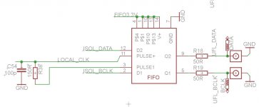
I don't see any significant change with it. But, at your schema, I see that the mclk termination resistor is 5.1R vs 51R. Is that wrong type or something else?
Hello Lemon,
Thanks for feedback.
Just to ensure : is the RC network is on the clock of the D latch, not on the D input ?
About damping resistor, please read post#22, akm appnotes use 5.1R for MCLK on 4495 and 90
You meant like something this?
The value of mclk terminations resistor was out of my mind...I had forgot it, completely! Thanks.
Hum...., I'm lost !
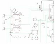
, what's that schematic ? your reclocker (external ) board ?If we do not consider UFL termination for now and only focus on the damping resistors (the 51 and 5.1R ones) and on the BICK delay, what I had in mind is drawn on the schematic attached
Attachments
Chris, sorry for the confused that I done to you.
I have applied a different but almost identical solution (I have describe it in post2) for our tests.
This is from a Potato 74AUC1G74 chips d-type flip-flops and works like 74AUP1G79.
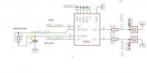
The RC network is on the pulse (from the local clocks), and feeds the pin 3 of this FIFO, this is correlated with the D1/Q1 (input bclk/output bclk).
From what I see from you schema, I have applied the same RC on 74AUC1G74.
Really, I try to find the area with the notes about termination resistors on AK datasheet and I can't find it!
Is that into AK4490 datasheet?
https://www.akm.com/akm/en/file/datasheet/AK4490EQ.pdf
I have applied a different but almost identical solution (I have describe it in post2) for our tests.
This is from a Potato 74AUC1G74 chips d-type flip-flops and works like 74AUP1G79.
The RC network is on the pulse (from the local clocks), and feeds the pin 3 of this FIFO, this is correlated with the D1/Q1 (input bclk/output bclk).
From what I see from you schema, I have applied the same RC on 74AUC1G74.
Really, I try to find the area with the notes about termination resistors on AK datasheet and I can't find it!
Is that into AK4490 datasheet?
https://www.akm.com/akm/en/file/datasheet/AK4490EQ.pdf
No problem !, I'll have a closer look to it later.
Link for app note, see page 42 :
http://www.akm.com/akm/en/file/ev-board-manual/AK4490EQ.pdf
Link for app note, see page 42 :
http://www.akm.com/akm/en/file/ev-board-manual/AK4490EQ.pdf
The RC network is on the pulse (from the local clocks), and feeds the pin 3 of this FIFO, this is correlated with the D1/Q1 (input bclk/output bclk).
From what I see from you schema, I have applied the same RC on 74AUC1G74.
If I understand yout schematic, MCK, BICK and DATA are coming from the left, and output ( to the AK4490) is on the right. If this is correct, in order to introduce a delay in BICK reclocking, the schematic must looks like this one
Attachments
Is your D latch a Potato Semi PO74G74A or a TI SN74AUC1G74 ?, because the TI one has a VCCmax of 2.7V, not 3.3. It's not supposed to operate properly above it's max specs. Potato is ok.
And both doesn't have Schmitt trigger input.... but if we leave this aside, the Potato has a ViH of 2V and the TI 1.7V so could expect a delay in the 5 - 10 nS range.
And both doesn't have Schmitt trigger input.... but if we leave this aside, the Potato has a ViH of 2V and the TI 1.7V so could expect a delay in the 5 - 10 nS range.
I'm a little behind on my part of the testing, but I did take a closer look at this "delay" of the BCLK coming out of our flip-flops.
It turns out that it is not a delay - it's just that some of the pulses have different period than others. This manifests itself like the "delayed" signal seen in lemon's screengrab.
Look at these two videos:
https://www.youtube.com/watch?v=nVRuWlQ5chY
https://youtu.be/YGXnZuIOqVE
Both of them are of the BCLK after its flip flop. The first one is of a 44.1K SR, the second one of 192K SR.
Notice how things change as I move the wave on the x and y axis.
I believe that this issue must be investigated and sorted out first.
Also, look at this capture of the I2S signal both before (channels 0, 1, 2) and after the flip flops (channels 4, 5, 6). Ignore channel 3, it was supposed to be the MCLK but my logic analyzer has nowhere near the required bandwidth to capture it properly:
https://ibb.co/j2u7oQ
This was done on an unpopulated dual ak4490 board, with just the flip flops for one channel soldered on. Signal source was an Amanero, MCLK was the Amanero's.
It seems that the signal is OK in that the LRCK does start at the falling edge of BCLK.
Also the reclocking seems to be helping the DATA signal.
In this case, the BCLK looks OK on the oscilloscope. No "ghosting" or anything.
But, what you are looking at is the beginning of the capture. After a few seconds things might be different - I didn't think to capture several seconds af data and scroll down a few seconds to see what happens. That is on my to-do list.
- Status
- This old topic is closed. If you want to reopen this topic, contact a moderator using the "Report Post" button.
- Home
- Source & Line
- Digital Line Level
- Arduino controlled dual mono AK4490 DAC