Hi there,
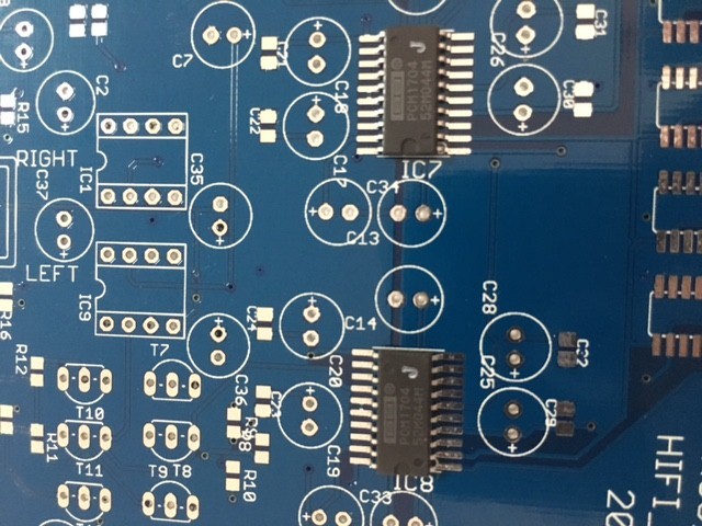
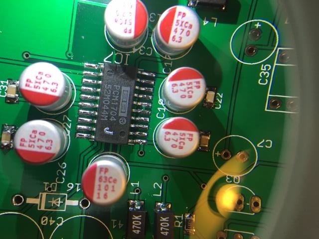
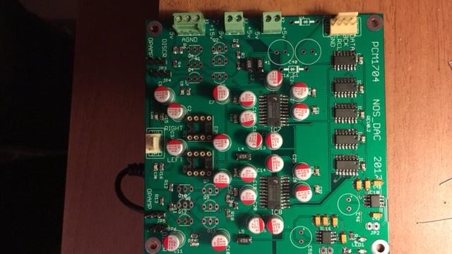
As Diy "buddy" group, we decided on pcm1704 without thinking about what is best in choosing a dac chip. Fortunately we found pcm1704 chip (j) on farnell.
This is first test video:
https://youtu.be/DJlK1UpE_c0
Details coming soon...
As Diy "buddy" group, we decided on pcm1704 without thinking about what is best in choosing a dac chip. Fortunately we found pcm1704 chip (j) on farnell.
This is first test video:
https://youtu.be/DJlK1UpE_c0
Details coming soon...


Thank you,Why TI stopped production of this fine dac ic?
Is internal structure influenced from pcm69 from BB or is it equivalent?
Nice project btw! Keep up the good work.
Really i am wondering too, why this chip's manufacture is stopped. Mostly old schooll hi end cd players had pcm1704. Maybe marketing strategy?
Maybe modern player's formats mismatches? But i really like its sound.
I think pcm63 is equivalent.
http://www.diyaudio.com/forums/digital-source/85468-replace-pcm63-pcm1704-dac-chip.html
Firstly, We have to finish all tests. Then, yes it will.Is the pcb available?
Hi,
We are assembling the cards. We will test it later. If everything works properly, there will be a few extra pcb.then I'll give you the info
Ok pm me if you can when available, ill buy one for sure.
I am about to start my own DAC design using the PCM1794. Looking at your PCB design I have a question, why ceramic capacitors are further away from the DAC pins then the electrolytics? The only benefit of using SMD ceramic caps is their low parasitic inductance (small size/leadless) which is important for supply pins bypass, but if they are connected to the IC pins with a long trace (high parasitic inductance) the single benefit they have is gone, IMO. Or maybe I'm missing something...?
Regards,
Oleg
Regards,
Oleg
Two options on pcb. selectable with jumpers. Discrete IV or Opamp IV. If we are sellect opamp we decided to use OPA627 or Burson V5.What opamps for I/V , output you using?
Hi oleg,
Normally, datasheet and other applications use only electrolitic capacitors. We use aluminyum organic polymer nichicon caps. These seramic caps only just to help. Possible, even if we don't use
Your PCM1794 design's dual mono, single chip stereo or non oversampling mode?
Normally, datasheet and other applications use only electrolitic capacitors. We use aluminyum organic polymer nichicon caps. These seramic caps only just to help. Possible, even if we don't use
Your PCM1794 design's dual mono, single chip stereo or non oversampling mode?


Two options on pcb. selectable with jumpers. Discrete IV or Opamp IV. If we are sellect opamp we decided to use OPA627 or Burson V5.
Ok thats good
Hi oleg,
Normally, datasheet and other applications use only electrolitic capacitors. We use aluminyum organic polymer nichicon caps. These seramic caps only just to help. Possible, even if we don't use
Understood. Thanks!
I just had a look at the PCM1704 datasheet and it shows the most misleading "typical application circuit" (Fig.5) that I've seen before. If you look carefully they indicate 0.1u caps in parallel to the 100u electrolytics on each supply pin. While 100u can be anywhere on the board (typically within 1"~2" from the DAC IC) the small 0.1u ceramic bypass caps should be as close to the supply pins as possible. This is indirectly stated on page 8. If you read other datasheets/app notes on high frequency circuits design then it will be clear why it should be done this way. Using polymer caps helps a bit but they are still inferior to ceramic caps at high (MHz range) frequencies. So if you plan another PCB revision you can position ceramic caps closer to the IC pins. Voltage reference pins do not need ceramic bypass since there should not be high frequency noise there. Also put 0.1u ceramic caps at each supply pin (to GND) of all op-amps. Fig.5 shows only one set but I guess it is meant for a skilled designer to fit the remaining parts. Adding a bunch of SMD capacitors pads in the right locations is easy. They can be left empty if not needed but can be very handy if you really need to fit a bypass capacitor there.
Your PCM1794 design's dual mono, single chip stereo or non oversampling mode?
I'll try a single chip stereo first and then see if I am satisfied with it or not before going further.
Regards,
Oleg
- Home
- Source & Line
- Digital Line Level
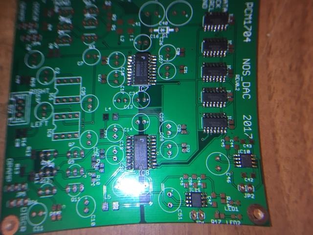
- PCM1704 Diy dac+ discrete i/v+ valve buffer