I use that xmos with the dac you have in Linux and no drivers needed.
Windows needs a licensed driver. Not sure about Mac...
As long as your os is Uac2 compliant then should be plug and play.
From the i2soverusb site their xmos board driver status is...
I2SoverUSB - I2S over USB Audio
Windows needs a licensed driver. Not sure about Mac...
As long as your os is Uac2 compliant then should be plug and play.
From the i2soverusb site their xmos board driver status is...
No drivers needed for Linux with UAC2 compliant kernel
No drivers needed for MAC OS version 10.6.4 and above
I2SoverUSB - I2S over USB Audio
The best you can do with this DAC is shown in:
Chinese ES9018K2M I2S DAC
Once you have to buy a new USB-I2S card anyway, perhaps consider:
HiFi ESS ES9028Q2M ES9028 I2S Input Decode Board Mill DAC Upgrade ES9018 amplifier DIY DSD IIS 32bit 384K /DSD64 128 256 512-in Amplifier from Consumer Electronics on Aliexpress.com | Alibaba Group
and
ATSAM3U1C XC2C64A Combo384 USB to I2S Digital Interface Refer to Amanero USB IIS Support DSD512 32bit 384K I2S Output for Audio-in Amplifier from Consumer Electronics on Aliexpress.com | Alibaba Group
The 5532 drops about 2-2.5V from each rail in the output. Which means maximum P-P voltage is about 5V less than supply voltage. With 9V supply the opamp supply is 7.7V, so the max voltage is quite limited, about 700mVRMS or 2.8V P-P.
The OPA2134 (not 2174) swings up to 0.5V of the supply rail, so is much more suited to these kind of conditions and circuits. You will get less distortion - it's simple maths really. It's not a fix for the inherent weaknesses of the board, but helps quite a lot in the running of it.
I am not sure where you got that 11.3 number from. The supply voltage to the board will always be 1.2-1.3V less than the power supply voltage, because that is the drop across the capacitance multiplier at the input of the power section. You are limited to an absolute maximum of 12V at the main supply node, because the 6.3V caps will then have 6V across them. Once you add the 1.2V back, you get 13.2V as the maximum possible input power supply.
If you toss those caps out and replace them with higher voltage units, you can push the main supply node to 15V, because that is the limit of the regulators powering the DAC chip. To remove that limitation, you have to make a significant number of changes and slowly approach the point of diminishing returns.
@eziitis, I will definitely consider the suggested boards. Re the change referred to for my existing DAC board, it's a bit over my current skills to implement.
@sangram, so the advantage of the 2134 is the much smaller voltage swing/drop from the supply rail thereby increasing the max voltage to about 6.+ V (?)
The 11.3V came from post#107. I think I understand your explanation re the limitations imposed by the 6.3V caps. But is there really any advantage in increasing the supply voltage from 9V to say it current maximum, and pushing it to say 15V if the caps are replaced - sound wise?
My own came, connected to a raspberry pi3, powered by direct power to 17V, there are no problems with 96/24 audio up, but the 44/16 will not work.
Who has the same problem with the 44/16, has it resolved?
I solved, by volume, forcing resampling from 16bit to 24bit.
@eziitis, I will definitely consider the suggested boards. Re the change referred to for my existing DAC board, it's a bit over my current skills to implement.
@sangram, so the advantage of the 2134 is the much smaller voltage swing/drop from the supply rail thereby increasing the max voltage to about 6.+ V (?)
The 11.3V came from post#107. I think I understand your explanation re the limitations imposed by the 6.3V caps. But is there really any advantage in increasing the supply voltage from 9V to say it current maximum, and pushing it to say 15V if the caps are replaced - sound wise?
I can't judge your present experience or use case, and have no way of working out if you will hear a difference, or by how much. Fact is I have never run the board that low, even with 12V supplies I faced some distortion at the highest volume levels (for example, when feeding an external preamp and pushing software volume to 100%).
If you have a very high gain setup and use software volume (and stay below say 50% of the dial) then no, you might not really benefit from any changes at least in measurements. Still, you are leaving quite a lot of performance on the table this way. It is ultimately up to you to see if you want to do it, and then make your own judgement on whether it was useful or not.
This might be an interesting read for people who have the ES9028Q2M board.
ESS ES9028Q2M DAC AD827版 I2S IIS入力 ★ 新製... - ヤフオク!
ESS ES9028Q2M DAC OPA627版 I2S IIS入力 ★ DC24... - ヤフオク!
ESS ES9028Q2M DAC AD827版 I2S IIS入力 ★ 新製... - ヤフオク!
ESS ES9028Q2M DAC OPA627版 I2S IIS入力 ★ DC24... - ヤフオク!
Hi everyone. I have a dilemma concerning the purchase of the ES9028Q2M board.
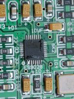
Some time ago I ordered a board that arrived with a solder bridge across two pins on the DAC chip (see photo). The seller initially tried to argue that it wouldn't affect the operation of the board. I refused to accept this, because the board had not been professionally assembled and obtained a full refund. I ordered a replacement board from a different seller, which arrived yesterday with exactly the same defect.
Has anyone had a similar problem?
Should I reject this one too? (Its becoming more trouble than its worth!)
Will the defect affect the operation of the chip? I can't find a pinout online , so I can't confirm this for myself.
Comments and opinions would be very much appreciated.
Attachments
Last edited:

That doesn't look like an accidental application of solder, and the one pin looks like a v ref of some sort, the other a ground. There isn't a bridge on any other pins?
Too bad that company doesn't provide data sheets, what a hassle.
Thanks for the reply.
I have attached a photo of the other board. As you can see the situation is identical. As far as I can see there are no other solder bridges on either board. I find it difficult to believe that this is just coincidence.
I can confirm that the two pins in question are connected to ground.
Has anyone else experienced a similar issue, and if so, does it affect performance?
Attachments
It is near 99% evident it is on purpose/design/normal that these 2 pins are bridged...
Anybody could help on this concern of mine : I want to modify the powersupply : I want to remove the capacitance multiplier (root supplies all board powers ?) which I have no real purpose for (don't like the associated voltage drop), in search of better efficiency (I use regulated buck supply as of now, and will continue to use a regulated one) : I am not sure of how exactly :
simply remove the 2 transistors : the small one and the big one and put a wire link between their most oppositive pins for each ?
Last edited:
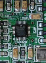
same as mine
An externally hosted image should be here but it was not working when we last tested it.

")
- Home
- Source & Line
- Digital Line Level
- Chinese ES9018K2M I2S DAC