Hi Hans,
thanks for sharing your experience and reporting your impressions. Nice job!
Glad you are so satisfied of the sonic results.
This remind me to my thought about digital audio: thinking the audio digital chain as a system, from the source to the analog section of the DAC, where the timing of the whole system is crucial.
Andrea
Hi Andrea.
Hmmm... thanks for your simulations and comments about the Driscoll vs. the Pierce. I'm not quite sure what the simulations may tell me - but I notice that the Driscoll's input waveform is asymmetrical - something I reckon is due to the transistor being used as an emitter follower ... (?) And that the Pierce's squarer output is a quite "nice" square wave")
I'm also thinking that the relatively high current levels in particularly the Driscoll oscillator makes for a good & stable PSU at the 6.144 MHz oscillator frequency. To this end I intend to change the 100 nF decoupling capacitor to a somewhat higher value (100 nF's impedance dip is around 12 MHz) that fits the 6.144 MHz frequency.
This greater p-p voltage wouldn't it mainly be in the start-up phase? If e.g. one starts up the Pierce slowly voltage-wise wouldn't it be possible to make it stay within the 5V voltages - so that it could be driven at the same level as the Driscoll?
This is entirely out of curiosity as I'm quite satisfied with the AT crystals I currently have - but in case you already know: What would the price for the HC-47/U be?
@Hans: Looks fine indeed - happy listening ;-)
Have a good day,
Jesper
Hmmm... thanks for your simulations and comments about the Driscoll vs. the Pierce. I'm not quite sure what the simulations may tell me - but I notice that the Driscoll's input waveform is asymmetrical - something I reckon is due to the transistor being used as an emitter follower ... (?) And that the Pierce's squarer output is a quite "nice" square wave
I'm also thinking that the relatively high current levels in particularly the Driscoll oscillator makes for a good & stable PSU at the 6.144 MHz oscillator frequency. To this end I intend to change the 100 nF decoupling capacitor to a somewhat higher value (100 nF's impedance dip is around 12 MHz) that fits the 6.144 MHz frequency.
Changing the values of some components (R1, C2, C3) one could increase the drive level, but there is the risk that the level at the input of the first inverter increases a bit, reaching a p-p voltage greater than the 5V supply rail, that's not a good practice.
This greater p-p voltage wouldn't it mainly be in the start-up phase? If e.g. one starts up the Pierce slowly voltage-wise wouldn't it be possible to make it stay within the 5V voltages - so that it could be driven at the same level as the Driscoll?
The final way could be to get a 3rd overtone SC-cut crystal at 6.144 MHz, that reachs a Q greater than 2M, but it will be very expensive since we should switch from HC-43/U to HC-47/U, that's more expensive.
This is entirely out of curiosity as I'm quite satisfied with the AT crystals I currently have
- but in case you already know: What would the price for the HC-47/U be?@Hans: Looks fine indeed - happy listening ;-)
Have a good day,
Jesper
@Hans:
I forgot this in my previous post:
This may be a solution but the clock that "shifts" the PCM1794 to my knowledge is the bit clock and it - presumably - is not affected by the shift registers. Whether in practice - i.e. beyond theory - the timing of the data signal to the individual PCM1794s affects the sound I do not know (I have a modified DDDAC myself).
Cheers,
Jesper
I forgot this in my previous post:
2.
the DDDac uses right justified mode.There are shift registers that cause jitter (please correct me, if I'm wrong). So get rid of these and implement shifting in the OS software
This may be a solution but the clock that "shifts" the PCM1794 to my knowledge is the bit clock and it - presumably - is not affected by the shift registers. Whether in practice - i.e. beyond theory - the timing of the data signal to the individual PCM1794s affects the sound I do not know (I have a modified DDDAC myself).
Cheers,
Jesper
@Jesper
Thank You for Your kind words and comment!
I think You are right. Although, in the dedicated thread for the DDDac it was reported that generating right justified mode via Botic OS and getting rid of that shifting rgisters (the whole mainboard) will lead to significant sonic improvements. It is not that easy to try that solution, for several parts and connections have to be desoldered. But I need to try, just to know... ;-)
In addition, I hope that You are right and there will be no improvement, for I plan to use the four i2s-lines (that BBB via Botic OS offers) to generate (again via Botic OS) a delay for the drivers of my multiway horn system. But generating right justified mode by OS would end in the need for one i2s-line per channel, so a four-way-delay would not be possible any more.
(As I am not too deep into linux, a delay via Botic OS will be a real challenge for me and any help would be appreciated very much. But being off topic, PM to this would be fine. Later I will try and find some help in the Botic support thread.)
Regards,
Hans
Hi Jesper,
the waveform at the base of Q1 is also affected by the diode clamp D1-D2, that limits the oscillation amplitude, to avoid overdriving the crystal. BTW, the output waveform before the squarer is a perfect sinewave (checked with oscilloscope), that's the most important thing.
A good and stable PSU is a must, you can easily increase the 100nF capacitance to 1uF.
Unfortunately is not very easy to increase the drive level of the crystal in the Pierce oscillator and keep the input of the first inverter below the supply voltage.
I have done several simulations changing the component values, but the input voltage of the first gate exceeds the power supply voltage. I'm not worried about the lower drive level because the picogate Pierce works in a different way at parallel resonance. In the Driscoll circuit we look for the highest loaded Q, that means the lowest impedance in the emitter circuit. This can be obtained increasing the bias of Q1, that typically means high drive level of the crystal.
The price of an SC-cut 3rd overtone in HC-47/U package at 6.144 MHz is around 70 Eur each and MOQ is 15 pcs. I requested a quote to Laptech some months ago (post #617).
Andrea
Hi Andrea,
Thanks again for your feedback and clarifications. I will then set myself to "peace of mind" with respect to the Pierce's drive level ;-)
Thanks also for the price on the SC-cut 3rd overtone in the HC-47/U package. I have missed this in #617. It is a somewhat different price so for now I'll be fine with the AT cuts.
Cheers,
Jesper
ecdesigns said:I assume that the goal is a low phase noise clock.
Here is an interesting article:
Clock Optimization: Analog Dialogue: Analog Devices
More gates in series, increased jitter, reduced SNR (Figure 16). In this case we have 3 HC gates in series and this adds up to approx. 6.6ps of jitter (see table 2).
There are off the shelf crystal oscillators that offer lower phase noise. One practical example would be the Tent labs crystal oscillator with specified 1ps jitter.
So why degrade a potential good clock design with 3 inverters placed in series?
All gates have tolerances in propagation delay, even when integrated on the same piece of silicon.
So paralleling gates results in temporary short circuits. The following zero’s and one’s represent output state change of 3 gate’s placed in parallel, switching at slightly different moments in time:
gate #1, 00001111
gate #2, 00111111
gate #3, 00000111
When all 3 signals do not have the same state at any given time, we create temporary short circuits.
0,0,0 = ok
1,1,1 = ok
1,0,0 = short circuit
0,1,0 = short circuit
0,1,1 = short circuit
1,0,0 = short circuit
1,0,1 = short circuit
1,1,0 = short circuit
The temporary short circuits will result in surge currents that pollute the power supply. I also have doubts if such a parallel buffer would be able to maintain specified 2.2ps jitter.
Good point already remarked in this thread.
From the theoretical point of view you are absolutely right, in the real world I'm not so sure.
I prefer talking about phase noise rather than about jitter, since jitter calculation depends on the integration bandwidth, while the phase noise is an absolute value related to the distance from carrier.
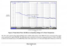
Please, take a look at the plot in the 5th post of this thread: paralleling 3 gates the Colpitts-Clapp oscillator shows a phase noise of -132dBc@10Hz from the carrier, that's a remarkable result compared with the plot showed in Tentlabs website, -93dBc@10Hz from the carrier. The Tentlabs is a 33.8688 MHz while the Clapp is a 11.2896MHz, so (maybe) it will perform around 9dBc better at 11.2896 Mhz, -102dBc or so. There is a substantial difference of about 30dBc.
So, or Herbert (the designer) was a very lucky man picking a IC where each gate is absolutely synchronized with each other, or the paralleling configuration does not matter much on the final result.
BTW, when I designed the first PCB, the Colpitts-Clapp, I followed Herbert's circuit including the paralleled gates. Then, this configuration was extended to the Driscoll oscillator.
The last designs, the TWTMC-P Pierce oscillator and the TWTMC_AIO combo Driscoll oscillators, use a single gate as the squarer.
I will make a revision of the Clapp and the Driscoll oscillator for the next batch, adopting the single gate squarer.
Andrea
BTW, when I designed the first PCB, the Colpitts-Clapp, I followed Herbert's circuit including the paralleled gates. Then, this configuration was extended to the Driscoll oscillator.
The last designs, the TWTMC-P Pierce oscillator and the TWTMC_AIO combo Driscoll oscillators, use a single gate as the squarer.
I will make a revision of the Clapp and the Driscoll oscillator for the next batch, adopting the single gate squarer.
Like Herbert said, it is important to have low output impedance for driving clock loads, a single gate won’t provide this. So the paralleling of gates seems logical.
However, what good is it to have say 50 Femto seconds of jitter while a clock buffer adds 6600 femto seconds of jitter.
The jitter spectrum is also -very- important. Two clocks with same jitter but different jitter spectrum can result in different DAC output spectrum and different related sound quality.
In a DAC we always have multiple modulated carrier frequencies that interference with the masterclock. This is one of the major uncorrectable flaws in digital audio, the more switching that is going on, the bigger the mess you get yourself into.
So keep in mind that a low phase noise masterclock is only one tiny piece of a large puzzle. There are many more flaws to tackle and this can take decades.
We could improve the clock buffer. Look for the low noise CMOS oscillator on this website
Low Phase Noise Design: Crystal Oscillators
The low noise CMOS oscillator has a single 74AC14 on the output. These have specified jitter of 0.99ps that is an improvement over 2.2ps of a 74HC04. But this will limit output power.
Even better would be removing the clock buffer alltogether. In this case we need something that can provide a low output impedance with sufficient drive capability like a transformer for example. We use it in tube amplifiers where we have a similar problem, driving a low ohmic speaker with a high ohmic output stage.
The difference between input and output impedance equals the transformation ratio squared. So with a 10:1 trafo we are talking about 100 times impedance reduction. With say 6K8 input impedance we can obtain 68 Ohm output impedance without using a buffer. Since we are using a transformer we can also have floating, galvanically isolated output(s) that eliminate unwanted ground loops and related degrading.
We can even add an extra isolated output for clocking an XMOS USB receiver for example while using digital isolators for the I2S signals. This way we have a clean clock at the XMOS and the DAC while maintaining galvanic insulation between both circuits.
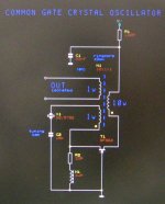
I attached a schematic of a grounded gate crystal oscillator circuit based on a 10:1 RF trafo. I measured approx. 10 Ohms output impedance without any clock buffer.
The next picture shows the transformer, two windings with one turn each and one winding with 10 turns.
So what do we have, a common gate circuit based on a BF862 (low noise RF JFET designed for car radio reciever front ends), low input impedance (source) and high output impedance (drain). Miller is not bothering us as we use a common gate circuit, bandwidth is maximum.
The drain (high Ohmic) drives the primary, don’t attempt to measure a signal here, it will stop oscillation. So keep this signal path as short as possible with lowest possible stray capacitance to GND.
The ac voltage across the primary will be around 20… 25Vpp depending on the VDS of the JFET. The circuit will protect itself (high Ohmic).
The 100 Ohm resistor is used to bias the JFET for linear operation and you may have to play with its value to find the right bias current as JFETs have tolerances. The 1uH choke in the source is necessary for oscillation (phase shift). You have to change its value depending on desired crystal frequency (lower frequency, higher value). This schematic is designed to operate around 23 MHz.
The crystal and feedback choke are connected between source and GND, the signal is attenuated and injected through the feedback winding (observe polarity or the circuit won’t oscillate).
The feedback winding offers low output impedance (transformation ratio) required for operating the crystal at series resonance for lowest phase noise.
The output signal is taken from the third winding, with this circuit you can expect around 2 … 2V5pp, sufficient to directly drive 3V3 circuits using a decoupled 1V65 voltage divider as reference. The secondary winding connects to this voltage reference and to the clock input. The clock input is held at 1V65 for optimal detection.
Over-driving an input will result in increased ground bounce and more unwanted harmonics, driving 3V3 logic with slightly lower 2 ... 2V5 signal avoids these unwanted issues.
The oscillator draws approx. 6mA @ 5V. It works at lower voltages too, but you may have to lower the value of the 100 Ohm resistor. This means battery powered operation is also possible.
Attachments
Last edited:
The low noise CMOS oscillator has a single 74AC14 on the output. These have specified jitter of 0.99ps that is an improvement over 2.2ps of a 74HC04. But this will limit output power.
Even better would be removing the clock buffer alltogether. In this case we need something that can provide a low output impedance with sufficient drive capability like a transformer for example. We use it in tube amplifiers where we have a similar problem, driving a low ohmic speaker with a high ohmic output stage.
There would be another way to convert the sine to square wave using a differential amplifier like the one suggested on the Wenzel website Waveform Conversion | but I believe the CMOS way using an inverter was the simpler and cleaner way. Please, take a look at the attached doc.
The output impedance of a 74HC04 should be around 40-50 ohm (I don't know about Potato unbuffered inverter, maybe it has lower output impedance). Is that enough low to drive the load? Surely it works, difficult to say if this increases phase noise (or jitter in time domain) without the suitable gear to test the results.
74AC04 and 74AC14 have lower output impedance, around 20 ohm at 3V3 if I'm not wrong, but the unbuffered types are not available.
Attachments
I can't find any "specified jitter" for CMOS or much else. Which is no surprise. All the references say that faster is better, except ECL has a low frequency noise problem.
What I did find was a reference that a 74HC164 has about 4 pS jitter and a 74AC164 about 1 pS.
Jitter is really a difficult parameter to use because of its "unbounded" nature. Phase noise vs. frequency is much more useful. For example 10 pS jitter on a 100 KHz clock is really good. On a 10 GHz clock it's catastrophic. And there are at least 3 specific types of jitter; cycle to cycle, etc.
I think the oscillator using a transformer is pretty neat. You would probably need a tuning network to get it to oscillate on the right harmonic etc. You are still at the mercy of the noise of the amplifier but you can optimize the coils for the best impedances for low noise. I would think a low noise wide band CFA (LME 49713?) might be very good in this implementation. However logic is not a nice linear load. It will draw a burst of current when the device switches. You also want a very fast slew at the input of the logic to minimize the impact of any noise in the system. Possibly a limited/clamped output swing.
Just as a reference here is the jitter measurement I made recently of a modest USB DAC (Xmos U8 AK4490 Audio HiFi Asynchronous USB Decoder DAC with Headphone Out PSU | eBay)
Its formatted as closely to the Stereophile measurements as I can with different hardware. Essentially free of jitter/phase noise artifacts. The unit has two small crystal oscillators of unknown origin. It also has very low distortion if you swap the original socketed opamp. I used an LME49720. If this is the baseline, it will be hard to improve upon.
I have measured some older premium DACs that were not as good but technology marches on and they aren't relevant any more.
Attachments
Like Herbert said, it is important to have low output impedance for driving clock loads, a single gate won’t provide this. So the paralleling of gates seems logical.
However, what good is it to have say 50 Femto seconds of jitter while a clock buffer adds 6600 femto seconds of jitter.
Out of all logic functions clock buffers generally have very low jitter. Not sure where the 6600fS comes from but it is certainly way off mark for a decent buffer. As an example ref to added phase noise graph of NB3L553 buffer. Very low added phase noise and that is at 100MHz. There are plenty
of others.
We can even add an extra isolated output for clocking an XMOS USB receiver for example while using digital isolators for the I2S signals. This way we have a clean clock at the XMOS and the DAC while maintaining galvanic insulation between both circuits.
I attached a schematic of a grounded gate crystal oscillator circuit based on a 10:1 RF trafo. I measured approx. 10 Ohms output impedance without any clock buffer.
It would be great to see phase noise measurements for this oscillator,
otherwise we don't really know, it certainly looks like a cool idea but I think measurements are needed to know.
Attachments
Jitter is really a difficult parameter to use because of its "unbounded" nature. Phase noise vs. frequency is much more useful.
That's the reason to talk about phase noise rather than jitter.
The bounds of the integration bandwidth affect heavily the result.
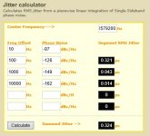
For example, if we calculate the jitter of the Crystek CCHD-957 at 22.5792 MHz from the phase noise plot included in the specs we get 324 femtoSec, because the lower limit of the integration bandwidth is 10 Hz.
If we calculate again the jitter adding a lower point, closer to the carrier such as 1 Hz, assuming 30dB worst than the point at 10 Hz (optimistic), we get 3.15 pS, that's an order of magnitude higher than the previous.
The higher the lower bandwidth limit, the lower the jitter. Increasing the lower bound any oscillator is similar to each other.
Phase noise vs frequency is an absolute value anyway comparable: the above Crystek shows a phase noise of -97dBc at 10 Hz from the carrier, there is no bounds issue.
Attachments
Last edited:
Hi all,
... Reading this buffer discussion I am wondering if it wouldn't be feasible to try to sort out "why & how" Herbert's oscillator reaches these low phase noise values with a seemingly simple output buffer/inverter?
1audio on a couple of occasions has mentioned that the "speed" of the buffer (IC?) seems to be a criteria and in terms of logic ICs most all of them are faster the higher their supply voltage ... And to this end - Herbert runs the 74HC04 off of 6.5 VDC - which even is beyond the "recommended operating conditions" for this IC ...
Isn't it possible that the reason why the 74HC04 performs with such low added jitter/phase noise (also?) is because its PSU voltage is 6.5 VDC? Might this e.g. reduce internal capacitances - or linearise something else?
To this end:
- Wouldn't it be feasible to consider how to "reduce" the output voltage of the 74HC04/74HCU04 in a "jitter adequate way" so that it may still be fed this high 6.5 VDC PSU voltage - yet its output is at a level where it's compatible with the most likely DACs/ADCs to be used (3.3 or 5 VDC logic levels)?
- Is it likely that other inverters - like e.g. the 74LVC04 type - will also show similarly - much - lower phase noise/jitter figures if it is fed from e.g. 6 VDC and not 3.3 VDC?
- And how about the FFs used in the TWTMC - D&D? Will they - similarly - benefit from a voltage that is close to - or maybe beyond - the recommended operating voltage?
To my memory the 6600 femto seconds was a reference to a specific IC's jitter figures ... Anyway, ecdesigns in a previous post listed some phase noise figures for various FF ICs (link courtesy triodehunter):
http://www.diyaudio.com/forums/digi...timate-weapon-fight-jitter-7.html#post2678005 (also #65 in the same thread)
and the figures are "way high" relative to what is output from Herbert's oscillator alone ... So IMHO this sentence:
is very relevant. Anyone has some experience here/suggestions in case a more traditional topology (a buffer) is used?
Cheers,
Jesper
... Reading this buffer discussion I am wondering if it wouldn't be feasible to try to sort out "why & how" Herbert's oscillator reaches these low phase noise values with a seemingly simple output buffer/inverter?
1audio on a couple of occasions has mentioned that the "speed" of the buffer (IC?) seems to be a criteria and in terms of logic ICs most all of them are faster the higher their supply voltage ... And to this end - Herbert runs the 74HC04 off of 6.5 VDC - which even is beyond the "recommended operating conditions" for this IC ...
Isn't it possible that the reason why the 74HC04 performs with such low added jitter/phase noise (also?) is because its PSU voltage is 6.5 VDC? Might this e.g. reduce internal capacitances - or linearise something else?
To this end:
- Wouldn't it be feasible to consider how to "reduce" the output voltage of the 74HC04/74HCU04 in a "jitter adequate way" so that it may still be fed this high 6.5 VDC PSU voltage - yet its output is at a level where it's compatible with the most likely DACs/ADCs to be used (3.3 or 5 VDC logic levels)?
- Is it likely that other inverters - like e.g. the 74LVC04 type - will also show similarly - much - lower phase noise/jitter figures if it is fed from e.g. 6 VDC and not 3.3 VDC?
- And how about the FFs used in the TWTMC - D&D? Will they - similarly - benefit from a voltage that is close to - or maybe beyond - the recommended operating voltage?
However, what good is it to have say 50 Femto seconds of jitter while a clock buffer adds 6600 femto seconds of jitter.
To my memory the 6600 femto seconds was a reference to a specific IC's jitter figures ... Anyway, ecdesigns in a previous post listed some phase noise figures for various FF ICs (link courtesy triodehunter):
http://www.diyaudio.com/forums/digi...timate-weapon-fight-jitter-7.html#post2678005 (also #65 in the same thread)
and the figures are "way high" relative to what is output from Herbert's oscillator alone ... So IMHO this sentence:
what good is it to have say 50 Femto seconds of jitter while a clock buffer adds 6600 (or ??) femto seconds of jitter.
is very relevant. Anyone has some experience here/suggestions in case a more traditional topology (a buffer) is used?
Cheers,
Jesper
Last edited:
a cmos inverter is noisy when operating in linear mode. we see two noise sources in paralell (reducing it) namely the Nchannel and the Pchannel input fets. operating them at higher currents helps reducing the noise voltage. as soon as a full swing is achieved the fets are not contributing to the noise anymore (other than bringing in supply and ground noise). that is when adding fast buffers does deteriorate the numbers.
nice,
the picture shows a 2T:10T design. is it a 4C65 core ?
coupling is not perfect, maybe split the 10T winding in two 5T with the 2T's in between ?
N30
B64290L44X830 - EPCOS - Transformer Cores, Toroid, Toroid, N30, 30.09 mm, 12.23 mm² | Farnell element14
I also thested these smaller versions (6.3mm) and no problems with these either, except it gets more difficult to locate all windings on such small former while maintaining minimum coupling capacitance.
B64290P37X830 - EPCOS - Transformer Cores, Toroid, Toroid, 6.3mm x 3.8mm x 2.5mm, N30, B64290P0037, 15.21 mm, 3.06 mm² | Farnell element14
This is N30 material too.
I use this oscillator for driving circuits on both sides of a galvanic insulation barrier (synchronous reclocking before and after magnetic pulse couplers).
So I need minimum capacitive coupling between the windings here. This configuration is used to eliminate ground loops between USB audio receiver and DAC.
I could not get the circuit to oscillate in ltspice. only at 2T:10T and by cascoding the jfet with a bipolar or same jfet . w/o the cascode, only at lower ratios. 1:2-1:3
Simulations are only as good as the parameters you enter, and you always forget some.
I built 3 of these oscillators and all oscillated without any problems. I did add a series resistor to the output for impedance matching and current limiting. When too high current is drawn (short-circuiting the outputs), oscillation could stop.
When higher output voltage is desired one can use two turns for the output winding.
Cascoding would limit voltage swing at the primary JFET drain, might offer some advantages, I will try that.
However, in audio circuits the cascoding of transistors would introduce a racing condition between two FETs or transistors that attempt to maintain equilibrium. One FET transistor equilibrium is disturbed by the other and vice versa.
This does not work out very well for audio circuits where it causes a gritty, overbright fatiguing sound.
I am not sure how this racing condition would translate to oscillator phase noise spectrum.
Up till now I had best results with oscillators based on a single JFET or transistor where such racing condition can’t occur because there is only a single servo.
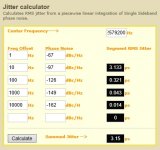
For example, if we calculate the jitter of the Crystek CCHD-957 at 22.5792 MHz from the phase noise plot included in the specs we get 324 femtoSec, because the lower limit of the integration bandwidth is 10 Hz.
If we calculate again the jitter adding a lower point, closer to the carrier such as 1 Hz, assuming 30dB worst than the point at 10 Hz (optimistic), we get 3.15 pS, that's an order of magnitude higher than the previous.
The higher the lower bandwidth limit, the lower the jitter. Increasing the lower bound any oscillator is similar to each other.
Phase noise vs frequency is an absolute value anyway comparable: the above Crystek shows a phase noise of -97dBc at 10 Hz from the carrier, there is no bounds issue.
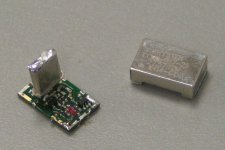
I tested Crystek CCHD-957 and the performance was simply lousy.
I opened one up to figure out what was causing it (picture).
Inside is a plain Pierce oscillator based on a NC7SZ00 logic gate and a NC7SZ126 buffer. That explains a lot, it’s hardly better than an integrated oscillator in a CPU.
I had much better results with cheap NDK or Epson oscillators (2.5 x 2mm SMD version).
The oscillators were tested in the same circuit running on the same clean power supply.
It was connected to a discrete Mosaic multibit DAC that directly drives high ohmic Beyer Dynamics studio headphones (DC-coupled passive pure resistive output, no semiconductors) . This combination reveals much more that audio sets that add coloration and noise. So if there is anything "wrong" with the master clock, this setup will reveal it immediately.
Attachments
strange, the N30 material hardly extends beyond 1Mhz, so the transformer is far from ideal and it's properties enter the equation. what could happen is that the active element is only active a very short percentage of the time, resulting in a low noise behaviour. the signal is then away from sinusoidial and symmetry..
- Status
- Not open for further replies.
- Home
- Source & Line
- Digital Line Level
- The Well Tempered Master Clock - Building a low phase noise/jitter crystal oscillator