any chance to use 45.xxx m and 49.xxxx m XOs?
It's a good idea from application POV but the phase noise starts to go to
billyo (down) sadly unless as 1Audio suggested start using phase locking
schemes. Gets complex. The best reasonably priced OCXO's I've seen at
50MHz seem to get max -110 dBc / 10Hz offset.
The Crystek 957 is actually very good at 45/49 Mhz at close to -100dB.
It seems there is a trade off especially in higher frequency oscillators for close in phase noise vs. broadband noise. The claim that the close in noise is important not substantiated at this time . . . but why not anyway? Higher frequency oscillators would be overtone oscillators, requiring more complex circuitry to get them working at the right frequency. Quickly this project gets more complex and difficult. A PLL with the right filtering to improve the HF oscillator using a good 4-6 MHz oscillator is quite involved. it would be fun but pretty time consuming and the results may not be worth the effort. Actually vibration may be come the dominant issue at the low frequencies. Its a well understood problem (try getting low phase noise on a helicopter) with some tricks for fixing it but better to avoid vibration sources.
The close in stuff actually may better be measured as short term stability deviations, actually easier than phase noise to measure.
The close in stuff actually may better be measured as short term stability deviations, actually easier than phase noise to measure.
On page 6 of this document http://www.euroquartz.co.uk/portals/0/pdf/tech-notes.pdf is an oscillator circuit for 3rd overtone crystals. It has a tunable inductor for suppressing the fundamental mode. Its a starting point for the oscillator. Also providing for a varactor diode in series with the crystal would allow tuning and even the basis for phase locking the oscillator. You can model this stuff in Spice. There are some crystal models that are pretty good and will allow some optimization before actual assembly and testing.
Dual XO & Dividers daughter board
I have attached a schematic diagram of a daughter board for the crystal oscillator.
It can accommodate two XOs and provides the logic to switch between them.
A dual coil latching RF relay is used to select the appropriate XO.
The switching device can be driven by two separate pulse signal or by a single low/high logic level (pulse or continuous signal). The pulse signal should be at least 15ms long. These two options have to be used alternatively.
As an option, you can power off the XO not in use by a second relay, driven by the same logic. Resistors R34 and R35 (0R0) have to be populated if the above option is not used.
The board provides also a divider network. The master clock can be divided by 2/4/8 and 16. If the dual clock utility is not used, R1 (0R0) must be populated, and K1, K2, all the logic and 12V supply should be removed.
There are also six inverters to delay the master clock, if it's used in conjunction with a divisor. For example, you could feed directly the BCK of the dac at 1.4112 MHz and sync back the source with delayed master clock at 11.2896 MHz.
The board provides 3 master clock outputs, direct or delayed, and 3 divided clock, to choice between the 4 options.
If you like a fully functional board with its power supply, I could include Demian's low noise regulators.
If there will be enough interest, I could develop the board.
Please, let me know.
Attachments
Andrea-
Good work. A few notes-
1) Crystal oscillators change a lot right after power on. Even ovenized oscillators show frequency shift and even phase noise shift right after power on. They improve over time, usually at least a week of continuous power to get stable.
2) Really good isolation of the power is important since even on really good oscillators its pretty easy to see modulation from supply ripple. Switching noise from logic is more insidious since its all synchronous but its still there. Also watch for ground noise getting back into the oscillators. The layout I posted was an effort to isolate the oscillators from all this stuff. I would do it differently today with surface mount parts but still the same concept.
3) Most DAC's are not sensitive to the clock/data phase alignment. It seems that general practice is essentially a set of D latches on the input to align the data and some other magic to make the chips pretty robust on problems with incoming data. I believe this is to accommodate relatively poor execution in commercial products. There may be a small benefit to alignment but it could be really elusive to find. For a really old DAC chip or an R2R chip local latches are important so the data transitions at the word clock edges don't get mangled by slightly off bit clock or data transitions. Keeping them shifted by a significant amount so nothing is happening at the clock edge is good practice.
- andrea_mori : 2 x 5.6448MHz + 2 x 11.2896MHz + 4 x PCB
- Eldam : 1 x 11.2896 Mhz + 4 x PCB
- esgigt : 1 x 11.2896 Mhz + 1 x PCB, soldered if possible
- fralippo : 1 x 22.5792 MHz and 1 x 24.576 MHz + 2 x PCB
- mravinsky : 2 x 11.2896 Mhz + 1 x PCB
- TNT : 1x22.5792MHz 1x24.5760MHz + 2 x PCB, soldered if possible
- 1audio : 1x22.5792MHz 1x24.5760MHz + 2 x PCB
- randytsuch : 2x25.0000MHz + 4 x PCB
- TNT or maybe : 1 x 11.2896 Mhz + 1 x PCB, soldered if possible
- myint67 : 1x11.2896mhz + 1pcb also soldered if possible
- EdwardTam : 2x 16.9344MHz + 1x PCB
- BDL : 1 x 11.2896 MHz + 2 x PCB
- thorstenlarsen : 2 x 11.2896 MHz + 2 x PCB
- Zoran : 1x22.5792MHz 1x24.5760MHz + 2 x PCB, (soldered or not...)
- walangalam : 1 x 11.2896 Mhz + 2 x PCB
- AR2: 1 x 22.5792 MHz and 1 x 24.576 MHz + 2 x PCB (soldering not needed)
- mcluxun: 1 x 22.5792 MHz and 1 x 24.576 MHz + 2 x PCB (soldering not needed)
- damohpi: 1 x 11.2896 + 1x PCB unsoldered
Updated list
- andrea_mori : 2 x 5.6448MHz + 2 x 11.2896MHz + 4 x PCB
- Eldam : 1 x 11.2896 Mhz + 4 x PCB
- esgigt : 1 x 11.2896 Mhz + 1 x PCB, soldered if possible
- fralippo : 1 x 22.5792 MHz and 1 x 24.576 MHz + 2 x PCB
- mravinsky : 2 x 11.2896 Mhz + 1 x PCB
- TNT : 1x22.5792MHz 1x24.5760MHz + 2 x PCB, soldered if possible
- 1audio : 1x22.5792MHz 1x24.5760MHz + 2 x PCB
- randytsuch : 2x25.0000MHz + 4 x PCB
- TNT or maybe : 1 x 11.2896 Mhz + 1 x PCB, soldered if possible
- myint67 : 1x11.2896mhz + 1pcb also soldered if possible
- EdwardTam : 2x 16.9344MHz + 1x PCB
- BDL : 1 x 11.2896 MHz + 2 x PCB
- thorstenlarsen : 2 x 11.2896 MHz + 2 x PCB
- Zoran : 1x22.5792MHz 1x24.5760MHz + 2 x PCB, (soldered or not...)
- walangalam : 1 x 11.2896 Mhz + 2 x PCB
- AR2: 1 x 22.5792 MHz and 1 x 24.576 MHz + 2 x PCB (soldering not needed)
- mcluxun: 1 x 22.5792 MHz and 1 x 24.576 MHz + 2 x PCB (soldering not needed)
- damohpi: 1 x 11.2896 + 1x PCB unsoldered
- noizas : 2 x 5.6448MHz + 2 x 11.2896MHz + 4 x PCB
- badrisuper : : 1 x 11.2896 Mhz + 2 x PCB
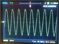
45.1584 MHz and 49.152 MHz 3rd overtone
Good news about higher frequency oscillator.
The attached schematic was modified to run a 3rd overtone crystal at 33.8688 MHz.
The tank circuit L4C2 is selected to be resonant at a frequency below the desired crystal harmonic (33.8688) but above the crystal`s next lower odd harmonic (11.2896), in this case the fundamental. Capacitor C9 acts as dc blocking.
For a 33.8688 MHz 3rd overtone crystal, C1 and C2 should be around 33pF and L4 1.2/1.5 uH.
The attached oscilloscope plot shows the sinewave signal. The Clapp oscillator runs at 33.8688 Mhz and the fundamental is suppressed.
It should run also at 5th overtone frequency, but I have no crystal to try.
Attachments
Updated list
- andrea_mori : 2 x 5.6448MHz + 2 x 11.2896MHz + 1 X 22.5792 MHz + 1 x 24.576 MHz + 1 x 45.1584 MHz + 1 x 49.152 MHz + 10 x PCB + 4 x daughter board PCB
- Eldam : 1 x 11.2896 Mhz + 4 x PCB
- esgigt : 1 x 11.2896 Mhz + 1 x PCB, soldered if possible
- fralippo : 1 x 22.5792 MHz and 1 x 24.576 MHz + 2 x PCB
- mravinsky : 2 x 11.2896 Mhz + 1 x PCB
- TNT : 1x22.5792MHz 1x24.5760MHz + 2 x PCB, soldered if possible
- 1audio : 1x22.5792MHz 1x24.5760MHz + 2 x PCB
- randytsuch : 2x25.0000MHz + 4 x PCB
- TNT or maybe : 1 x 11.2896 Mhz + 1 x PCB, soldered if possible
- myint67 : 1x11.2896mhz + 1pcb also soldered if possible
- EdwardTam : 2x 16.9344MHz + 1x PCB
- BDL : 1 x 11.2896 MHz + 2 x PCB
- thorstenlarsen : 2 x 11.2896 MHz + 2 x PCB
- Zoran : 1x22.5792MHz 1x24.5760MHz + 2 x PCB, (soldered or not...)
- walangalam : 1 x 11.2896 Mhz + 2 x PCB
- AR2: 1 x 22.5792 MHz and 1 x 24.576 MHz + 2 x PCB (soldering not needed)
- mcluxun: 1 x 22.5792 MHz and 1 x 24.576 MHz + 2 x PCB (soldering not needed)
- damohpi: 1 x 11.2896 + 1x PCB unsoldered
- noizas : 2 x 5.6448MHz + 2 x 11.2896MHz + 4 x PCB
- badrisuper : : 1 x 11.2896 Mhz + 2 x PCB
Last edited:
As anyone contemplated on how to "fit" these on a Ian clock board?
//
You can use u.fl. cable or try to fit it directly removing the XO sockets from the clock board.
Another option could be to fit it close to the DAC and send back the master clock to Fifo board via u.fl. cable.
Good news about higher frequency oscillator.
The attached schematic was modified to run a 3rd overtone crystal at 33.8688 MHz.
The tank circuit L4C2 is selected to be resonant at a frequency below the desired crystal harmonic (33.8688) but above the crystal`s next lower odd harmonic (11.2896), in this case the fundamental. Capacitor C9 acts as dc blocking.
For a 33.8688 MHz 3rd overtone crystal, C1 and C2 should be around 33pF and L4 1.2/1.5 uH.
The attached oscilloscope plot shows the sinewave signal. The Clapp oscillator runs at 33.8688 Mhz and the fundamental is suppressed.
It should run also at 5th overtone frequency, but I have no crystal to try.
Looking at the circuit I think the 20K bias resistor for the JFET will limit the noise. The noise of the transistor modulates the oscillator, which is why you want low noise transistors for this function. The 20K resistor at 18 nV/rtHz will be much higher than the transistor. The transistor is listed as 6 nV/rtHz. There is no other low Z impedance in parallel so the 20K will define the noise. You really want that to be low. I suspect using an inductor + resistor of around 100 Ohms + 10 uH may be enough and will drop the close in phase noise a lot. It might work with just an inductor.
You can use u.fl. cable or try to fit it directly removing the XO sockets from the clock board.
Another option could be to fit it close to the DAC and send back the master clock to Fifo board via u.fl. cable.
Hmm, if you want both clock freq. regimes...
//
Hmm, if you want both clock freq. regimes...
//
I presume Ian's FIFO board detects the sample rate and provides a signal to switch between the 2 frequencies. I'm note sure, since I have never seen any detailed schematic.
If so, the Dual XO & Dividers daughter board could do the job, syncing back via u.fl. cable.
Looking at the circuit I think the 20K bias resistor for the JFET will limit the noise. The noise of the transistor modulates the oscillator, which is why you want low noise transistors for this function. The 20K resistor at 18 nV/rtHz will be much higher than the transistor. The transistor is listed as 6 nV/rtHz. There is no other low Z impedance in parallel so the 20K will define the noise. You really want that to be low. I suspect using an inductor + resistor of around 100 Ohms + 10 uH may be enough and will drop the close in phase noise a lot. It might work with just an inductor.
You mean R1? If so, it is 220K. It acts as the AGC (leakage current).
To replace it with an inductor, we need high reactance, for example around 3mH at 11.2896 MHz and about 700 uH to 49,152 MHz.
In addition, it remains to check what happens in DC.
- Status
- Not open for further replies.
- Home
- Source & Line
- Digital Line Level
- The Well Tempered Master Clock - Building a low phase noise/jitter crystal oscillator