I posted this by accident on another thread anyway here it should be.
Funny you should bring up the AD844 Jan.
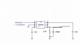
I found this circuit of Pedja Rodic's (attached) and used it as is (NO FEEDBACK) and it worked a treat, best opamp based I/V so far by a long way, it blew the OPA627 completely away I though it would never be beaten except for a discrete I/V of some sort. (And I’ve tried just about every opamp out there)
I used it without feedback as per the diagram and was very very happy. Used with TZ as he has it 1.5K with 1000pf to ground, I think this gives a 1st order rolloff –3db @100khz.
Does the 1.5k resistor have a bearing on what input resistance the dac (PCM1704 in my case) sees?
Because I changed the resistor for 2.2k to get some more gain but this time with a 260pf cap –3db @ 270khz (still all nice and stable with a bit more gain) still very very good.
But I had the feeling it was puchier and more dynamic with the 1.5k resistor even though I had less gain. I feel that the input loading for the PCM1704 is better with the 1.5k than the 2.2k resistor or am I imagining things?.
Cheers and thanks for your input George
Hi George,
I want to apply this solution for my TDA1541A DAC.
Could I use a VR, say 3K ohm, instead of 1.5k resistor at TZ pin as a volume control for the DAC? I want to connect the DAC to power amp (sunfire 300) without a preamp. Is it possible? Can I have your advises this case?
Thanks and Regards
Can't see why not, just use a 220pfcap across it for a -3db at 241khz. Watch you don't overload the input of the sub with too much gain.
Cheers George
Last edited:
Glad to see this thread being alive again ^_^
This IV resistor is critical. IMHO, using a VR may not be an optimal solution. Besides that, you need to look into Sunfire's input biased current. This setup could be too weak to drive an amplifier when VR is at low resistance.
This IV resistor is critical. IMHO, using a VR may not be an optimal solution. Besides that, you need to look into Sunfire's input biased current. This setup could be too weak to drive an amplifier when VR is at low resistance.
Glad to see this thread being alive again ^_^
This IV resistor is critical. IMHO, using a VR may not be an optimal solution. Besides that, you need to look into Sunfire's input biased current. This setup could be too weak to drive an amplifier when VR is at low resistance.
The Sunfire has the RCA Input impedance of 24K ohm (from the manual)
Now, I use 22 ohm as I/V resistor then a SRPP 6Dj8 tube buffer which has gain of 25, output resistor of 500 ohm and Pmax of 0.9W. I want to insert AD844 as a IV stage (replacing for I/V resistor) and BTW a volume control here. The reason for doing that is to remove the next preamp from the system.
I want to remove the SRPP tube buffer and use 844 as a buffer too. However I do not see where to insert the VR here this way
I am a newbie, please advised me.
Thanks a lot.
Hi 4rgroup,
I've never thought about that. I think the performance will greatly affected by the quality of VR and the wiring. You can try to use the VR on pin5 and take pin6 as the output to the amplifier. If you don't take pin6 as the output, an external buffer is recommended. There are many options here. You may read other's feedback on this thread.
Poting
Can't see why not, just use a 220pfcap across it for a -3db at 241khz. Watch you don't overload the input of the sub with too much gain.
Cheers George
Dear George,
I have only one AD844 so far. So I've turned to Discrete Diamond Non-Feedback I/V Stage circuit (DDNF) as a I/V stage in my DAC.
It's schematics can be found here: http://www.diyaudio.com/forums/blog...-out-production-pedja-rogic-ddnf-iv-stage.pdf
I aslo use a SRPP SRPP 6Dj8 tube as the gain stage. The TDA1541A’s output phase is inverted (am I right?) and the SRPP gain stage inverts the phase too. If the DDNF's phase is not inverted, the DAC as a whole has correct polarity.
My question is that the DDNF's output phase is inverted or non-inverted. Could you kindly advise me.
Thanks and Regards.
Last edited:
Currently I have had a BUF03 as buffer, but I want to replace it. I also want to make a balanced driver.
Many have used the OPA627.
I see that the OPA1612 is newer and part of the SoundPlus family of opamps - and more widely available. Both are unity gain stable.
What are your experiences.
Should I be aware of fakes (some Ali prices are lower than others)?
Many have used the OPA627.
I see that the OPA1612 is newer and part of the SoundPlus family of opamps - and more widely available. Both are unity gain stable.
What are your experiences.
Should I be aware of fakes (some Ali prices are lower than others)?
Last edited:
Glad to see this thread being alive again ^_^
This IV resistor is critical. IMHO, using a VR may not be an optimal solution. Besides that, you need to look into Sunfire's input biased current. This setup could be too weak to drive an amplifier when VR is at low resistance.
What about using a variable resistor at 1k5 (the intended I/V value) and then just using the tap as volume control?
The wiper must be loaded high (for optimal response) otherwise there will be sagging at higher volume settings.
That apart from the quality of course, but some studio VR could have a high non-inductive quality I expect.
yeah I mentioned someone should try this 6mts ago.
Cheers George
In the 844 you have two parts, you have the OTA front-end and in the 844 it runs at a fixed current and I estimate it might be only 2mA. By stacking the 844, the OTA has a lot more current, not just the other part, the buffer. In the 861 you can set it by a single resistor and easily run 3-4 times the current through the OTA part.
Mind you, the 861 is really meant for low -/+5V operation and the 844 can handle -/+15V and a bit more OK. So there are more variables there.
Cheers, Joe
I am interested in the current passing through the transistors on the inputs of the AD844 to determine its limits in class A.
Is it reasonable to guess that there are three paths of equal current between the power supplies... excluding the output stage? Two paths on either side of the input quad and a current mirrored from the inverting terminal? If the output stage current is included in the total current of 6.5mA this suggests perhaps 1.5mA in each of the three legs. This is dependent upon the output stage buffer current consuming 2mA. Is the actual current information available anywhere?
Cheers,Gerrit
Hi Joe,
My reason for asking is to determine if the AD844's input stage has enough class A current capability that it can be used as an output buffer in lieu of a BUF03 or the AD844's normal output buffer. In other words using only the input stage of a second AD844 with input to pin 3 and the output taken from pin 2, with its Tz pin 5 connected to ground.
From the thread the output buffer in the AD844 isn't necessarily a good one. Having done experiments with and without the AD844's output buffer it appears susceptible to oscillation of the kind that can become rectified and reflected back into the audio range. Given that oscillations normally occur under feedback conditions it would seem that the current limiters in the output buffer can be responsible. In other words, if high frequency transients exist at the Tz node, as either coming from the input, from the power supplies, or from ground through the RC network that members are connecting to this node, this can affect or activate the current limiters. This necessitates a requirement for good power supply decoupling and general high frequency network considerations in any design. Ultimately the output buffer in the AD844 is a feedback amplifier.
The AD844 has already proven itself as an excellent device by members for use as an I/V converter, one that uses a unity gain input buffer. Given that the input buffer doesn't employ current limiting (as indicated by the data sheet warning not to exceed 5mA on the inverting terminal) it isn't considered prone to oscillations.
Another factor is that the input buffer is designed to be clean (being laser trimmed as well), as the voltage across the input terminals represent the reference points that generates feedback, hence are outside the feedback loop (the AD844 can't guess what needs fixing). This is not the case for the class AB output buffer, normally current limited to protect the device from damage, with feedback limiting its non-linearity.
Cheers, Gerrit
Quick couple of questions on the 2019 status of this amazingly interesting thread:
Are the newest designs still using a JFET current source circuit on the input? Is this necessary if the output is capacitively coupled? Would modern, in-stock JFETs like the MMBF4393 or 2SK3666 be appropriate since 2SK170s are somewhat expensive at this point?
If one were to forego the OPA627, would a BUF634 be acceptable for a TZ-output arrangement since BUF03's are now also very expensive? I know it's bipolar, but the datasheet says 80Mohm input impedance or 8Mohm in high-BW mode. 80M in parallel with 1.5kohm shouldn't cause much of an issue, right?
I fear the 844's output buffer might not be able to drive much capacitance, especially the ~100pF/m of some RCA cables and that could be causing some of the sound quality issues seen here using pin 6 directly.
Last edited:
I fear the 844's output buffer might not be able to drive much capacitance, especially the ~100pF/m of some RCA cables and that could be causing some of the sound quality issues seen here using pin 6 directly.
Forget the AD844's own buffer it's not very good sounding. Come off the 844's pin5 to your own buffer, I found a "genuine" OPA627 to be exemplary, make sure it's genuine by getting it from an authorized TI distributor, as there are many fakes of these.
Forget the BUF03 in the pic that's the first one I tried, too dirty sounding great bass though.
Cheers George
Attachments
Last edited:
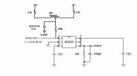
George,
Are we still using the input bias current source? I noticed your recent schematics (including the one you just posted) don't have one.
With the above 844 using pin 5 and the OPA627 and small amount dc offset can be trimmed out using the OPA627's offset adjustment.
But if you have a large amount of dc offset coming from the dac thewn you need to use this setup to trim it out.
Cheers George
Attachments
If its a line level application then presumably noise isn't a major issue, in which case a SSM3K35 will out-perform an SK170 in practically every other electrical parameter besides noise, breakdown voltage and threshold voltage stability. Its a MOSFET (enhancement mode) though, not a JFET so will need circuitry changes. It is a lot cheaper than a K170 but only available in SMT.
If anyone's interested in a DAC unity gain buffer, I use this one on my 'lingDAC' design. Its using another modern Toshiba MOSFET, SSM3J327 which gives it a very low Zout for a source follower because the FET's transconductance is so high. Mouser has them in stock right now but they do tend to sell out fast....
SSM3J327R,LF Toshiba | Mouser
SSM3J327R,LF Toshiba | Mouser
Attachments
If anyone's interested in a DAC unity gain buffer....
Thanks very much.
")
- Home
- Source & Line
- Digital Line Level
- Using the AD844 as an I/V