hmm mate both have their drawbacks, think I like 1 better but its not ideal either. both are very cramped. can you rotate the BIIISE 90 degrees clockwise in layout 2 and sit the dac outs pretty much directly over the inputs? that way the control wires dont cross over all the analogue stuff, the current outputs especially, i2s lines are only marginally longer and with the acko iso they are driven anyway so length is not as much an issue. seems a lot to be running from a single 5v secondary.
Sorry, I'm confused?
what about? I dont think I can put it another way, the isolator has an input power supply and an output power supply, both LDOs are on the board, just need to supply raw DC for input and output sides, output side should probably come from, or be grounded at the dac. input side should come from somewhere else ir the isolator is a bit pointless, maybe from amanero itself its 5v output (direct from USB power, not regulated except on the ISO board)
Last edited:
what about? I dont think I can put it another way, the isolator has an input power supply and an output power supply, both LDOs are on the board, just need to supply raw DC for input and output sides, output side should probably come from, or be grounded at the dac. input side should come from somewhere else ir the isolator is a bit pointless, maybe from amanero itself its 5v output (direct from USB power, not regulated except on the ISO board)
Yeah sorry, whats left of my brain is fried, it was 45C here today. I thought you were responding to my layout.
Thanks for the input, I'll ponder the options
thanks again
Before I get too far again I would greatly appreciate any input on the latest iteration. I have tried to get a good Jpeg that you can view from the thread but the only way I can get a reasonable quality is to save it as a pdf. There are a lot of bits that are not connected in this version but it is the general layout that matters. I have taken the advice given, to do this I had to make the case bigger than originally planned. I have added an OTTO to switch between the 2 SPDIF inputs. I'm not completely sure how the Isolator reclocker is to be wired to the BIIISE, or how the OTTO connects to the Mega or do I connect it to the BIIISE?
Attachments
Hi DQ,
Looks good to me (I did originally comment on SNA but since qusp is replying over here it might be more logical to keep all comments on here, perhaps).
One thought, are you limited to height of the enclosure?
It may be worthwhile pulling the IV stage higher and slide the BIII-SE underneath it and shorten the BIII outputs even more. You could then stack the arduino level shifter above the arduino board and run longer lead wires for the spdif switching into the enclosure, say on the 'front' side of the BIII-SE rather than currently close to the back of the enclosure and pull the case narrower if you wanted? That way the amanero board would be on one side and the otto would be on the other side of the BIII. Does that make sense? It has been a long day here so I might not be as clear as otherwise :/
What dimensions of the enclosure are more critical to you? Height/width/depth?
Cheers,
Chris
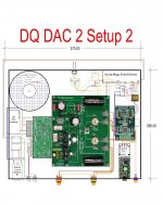
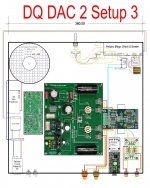
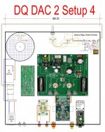
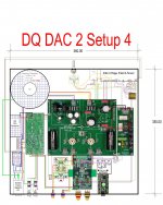
This is the best I can do re resolution, here are versions 2, 3 & 4
hochopeper
I caught your advice on SNA & applied to to one of the versions, It's getting confusing")
I'll read through your last post after I post this, thanks
Setup 4 looks the best to me as long as having long I2C lines to the BIII from the Mega isn't a big problem.
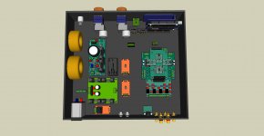
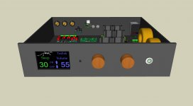
The idea with the Mega is to have it at the front corner as per the Sketchup Jpeg so I can connect the USB with ease in the future, the Sketchup Jpeg is of DQ DAC 1 which is playing at the moment but still in it's prototype cloths as per the photo.
hochopeper
I caught your advice on SNA & applied to to one of the versions, It's getting confusing
I'll read through your last post after I post this, thanks
Setup 4 looks the best to me as long as having long I2C lines to the BIII from the Mega isn't a big problem.
The idea with the Mega is to have it at the front corner as per the Sketchup Jpeg so I can connect the USB with ease in the future, the Sketchup Jpeg is of DQ DAC 1 which is playing at the moment but still in it's prototype cloths as per the photo.
Attachments
-
 13-01-19 DQ DAC 2 Setup 2.jpg411.5 KB · Views: 365
 -
 13-01-19 DQ DAC 2 Setup 3.jpg478.3 KB · Views: 336
 -
 13-01-19 DQ DAC 2 Setup 4.jpg305.1 KB · Views: 333
 -
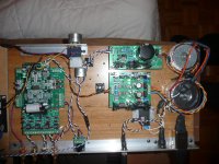
 12-11-23 DAC-Arduino Build Top.jpg343.4 KB · Views: 337
 -
 12-10-29 Arduino Control01_1.JPG651.7 KB · Views: 327
 -
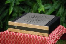
 12-12-07 DQ DAC 1.jpg233 KB · Views: 210
 -
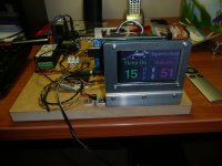 12-09-09 Arduino Touch Screen01_3.JPG499.9 KB · Views: 182
Last edited:
I was wrong the dimensions of Setup 3 & 4 they are fine 360W x 355D the internal height needs to be kept to 75mm as the finished design needs to be no bigger than one of the amps I built.
If I move the BIII under the I/V stage it's going to make getting to things difficult & I hate that
If I move the BIII under the I/V stage it's going to make getting to things difficult & I hate that
Attachments
Last edited:
And the tooooooobs out the top of the 75mm enclosure or included in the 75mm?
I am familiar with the aussie amps enclosures that you built from your SNA thread but man they look good, still. Didn't know they were 'only' 75mm tall. I just received some 151mm x 300mm conrad heatsinks arrive here this week for my next amps
I am familiar with the aussie amps enclosures that you built from your SNA thread but man they look good, still. Didn't know they were 'only' 75mm tall. I just received some 151mm x 300mm conrad heatsinks arrive here this week for my next amps
And the tooooooobs out the top of the 75mm enclosure or included in the 75mm?
I am familiar with the aussie amps enclosures that you built from your SNA thread but man they look good, still. Didn't know they were 'only' 75mm tall. I just received some 151mm x 300mm conrad heatsinks arrive here this week for my next amps
I like the idea of the Toooobs out the top but I dont think it's going to happen, fortunately the tubes are only 45mm high (Full Music 12AX7)
The heat sinks I used are only 75mm high x 350mm long.
What type of amps are you going to built, A class by the size of the heatsink
Well I think this is it, if you see anything obviously wrong I would love to hear from you.
I was wondering about the grounding, at this stage the only things connected to the Earth point are the Earth AC Input & the Shield from the larger trannie, should anything else go back to the earth point?
I haven't finished the wiring for Acko's isolator reclocker as I'm not sure how it's wired.
I think everything else is done.
The PDF is much better quality
Attachments
Last edited:
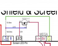
I want to dim the LED backlight to the screen I will be using, in the past I used the Arduino PWM output with a resistor in series to dim the backlight.
The manufacturer says I should ideally be using a transistor to do this & was kind enough to send me a mud map of how to go about it.
In the drawing below I have shown what I think I should do to make this work but I am not sure I have got it right.
The theory is that the LED backlight is supplied via the Drain & the Collector is supplied by the Arduino 3.3v output.
The gate voltage is dropped from 5v to 2.1v by the voltage divider and the gate voltage is pulsed using the PWM function to turn the transistor on and off, the frequency of the PWM is changed to dim the LED.
Can anyone confirm I have this right
Attachments
12v trigger out
Hi DQ828,
I've been following your build with interest and been trying to work out what components you are using to provide the 12v trigger out. I'd like to get my power amp to switch based on the DAC/pre I'm building. I can see that you've got a 12v feed from the transformer but what happens after that?
Thanks for any help,
Crom
I want to dim the LED backlight to the screen I will be using, in the past I used the Arduino PWM output with a resistor in series to dim the backlight.
The manufacturer says I should ideally be using a transistor to do this & was kind enough to send me a mud map of how to go about it.
In the drawing below I have shown what I think I should do to make this work but I am not sure I have got it right.
The theory is that the LED backlight is supplied via the Drain & the Collector is supplied by the Arduino 3.3v output.
The gate voltage is dropped from 5v to 2.1v by the voltage divider and the gate voltage is pulsed using the PWM function to turn the transistor on and off, the frequency of the PWM is changed to dim the LED.
Can anyone confirm I have this right
Looks OK
yes, unless you are actually using the amanero clock for clocking the BIIISE the reclocking mod is totally superfluous. the BIIISE already uses its onboard clock to not only control the dac, I believe it has some flipflops that reclock the incoming bck/lrck/sdata now. you can see them directly after the i2s inputs IC5.ICx, ICx on D2, D1, DCK.
There are no re-clocking flip-flops on the Buffalo. When using the onboard 100MHz XO (asynch), re-clocking the input clocks is a bad idea. It basically makes it impossible for the internal jitter elimination to function properly.
Those chips are analog switches for controlling the input selection (I2S/DSD or S/PDIF).
Hi Brian,
From the BIIISE highlights on the website :-
"High-precision, ultra-low-phase noise clock and integrated reclocking".
There is some confusion in a number of threads here on DIYAUDIO leading to the incorrect assumption that the analoge switch chips are Flip Flops
I appreciate you can connect and external clock but what does "integrated reclocking" mean exactly ?
.
Hi Brian,
From the BIIISE highlights on the website :-
"High-precision, ultra-low-phase noise clock and integrated reclocking".
There is some confusion in a number of threads here on DIYAUDIO leading to the incorrect assumption that the analoge switch chips are Flip Flops
I appreciate you can connect and external clock but what does "integrated reclocking" mean exactly ?
.
It is one of the features (patented) of the ES9018 chip.
RMAF11: Digital Jitter and Volume Controls, Martin Mallison, CTO, ESS Technology - YouTube
Fast forward to 16:00.
It is one of the features (patented) of the ES9018 chip.
RMAF11: Digital Jitter and Volume Controls, Martin Mallison, CTO, ESS Technology - YouTube
Fast forward to 16:00.
Thanks Brian.
Wish I had seen this video a while back.
So the 9018 data sheet shows a DPLL that does not exist ! (and a set of DPLL registers that do exit)
The "DPLL" is more like an advanced ASRC.
I always wondered by MCLK was not a multiple of FS.
This stuff is sinking in slowly.
Martin Mallinson sounds like he comes from only a few tens of miles North of me.
Pity he has moved away, I would gladly buy him a few beers over a chat.
When you say "re-clocking the input clocks is a bad idea" I gather you mean
in relation to 9018 MCLK, not just "cleaning up the edges" in relation to the transport clock.
Thanks again for the information.
Last edited:
There are no re-clocking flip-flops on the Buffalo. When using the onboard 100MHz XO (asynch).
Those chips are analog switches for controlling the input selection (I2S/DSD or S/PDIF).
OK thanks for clearing that up. it seems i'm not the only one that misread your claims of a reclocker as something external to what exists in the ESS dac itself, it is certainly framed as such; whether intentional or not it reads as a new feature that you have implemented; rather than something that has not changed since the Buff32.
that is your opinion.re-clocking the input clocks is a bad idea. It basically makes it impossible for the internal jitter elimination to function properly.
You can also look at it in the way, that if there is nothing for it to do, because the input jitter is no more than that of the very low jitter clock and flip flop in series, it can only add error (even if it is silly small error), so the best result is actually that it doesnt know what to do and does nothing IMO.
That is kind of the point of things like the fifo, to take responsibility for these functions and delete the crossing of clock domains altogether, making the transport and dac temporally one.
at the very least it gets rid of the ESS warm up time for dropouts on hires material. there is no more data to show it is detrimental than beneficial.
I've seen that video several times already, its quite interesting, he does waffle a bit, but in general I agree with most things he says and understand he has to pander to the audiophile masses somewhat with some of the language and make some stuff up for what parts even they dont really fully understand.
However it is their stance that the ESS is essentially faultless in every way, in everything it does. that is not the case, it seems unusually sensitive to jitter on BCK, it seems unusually sensitive to ripple on ground in Async mode, the digital filter is not perfect and the MUX is a bit bunky and it is not source agnostic in my experience with both your ESS dacs and Ackos.
I still prefer it over everything ive tried when used as a DAC only and will continue to use it for the foreseeable future, but I do believe that some of the integrated functions are now better served by more modern solutions to help it along. software or FPGA apodising digital filter, synchronously clocked buffered source/transport and external DSP are all better now ~4 years later.
the ESS reclocking scheme is very good and was revolutionary at the time, but I do believe it has been superseded.
you of course are rational to go with what your experience tells you just as I am. I do not believe either way is specifically wrong.
Last edited:
- Status
- This old topic is closed. If you want to reopen this topic, contact a moderator using the "Report Post" button.
- Home
- Source & Line
- Digital Line Level
- DQ DAC 2, BIII SE, Tube-I-Zator, Arduino, Amanero Build