Most people have joined their shunt regs to the connection points for the existing LF regulators. Because these regulators are surface mount, there aren't holes that go all the way through, only pads on the top of the board.So, is plenty of room to install the shunt but nobody use it... maybe have some contraindication?
The connection should not be a problem as the space... if some millimeters more are needed I can use higher standoff. Maybe the hot dissipation?
Regards,
Enrico
Of course you can use the holes from some of the electrolytic caps and mount underneath, but you will need to run some wires for the input voltage to the shunts
Most people have joined their shunt regs to the connection points for the existing LF regulators. Because these regulators are surface mount, there aren't holes that go all the way through, only pads on the top of the board.
Of course you can use the holes from some of the electrolytic caps and mount underneath, but you will need to run some wires for the input voltage to the shunts
Thanks James.
Due to the fact that the electrolytics are to be dismounted maybe can be a good option to mount them under the board... I will understand better when I will get the tents in the hand and I will let you know.
Regards,
Enrico
An externally hosted image should be here but it was not working when we last tested it.
In an attempt to understand what Rick and Supersurfer are discussing, I drew up this picture. Is this what is being proposed?
Any comments?
I would do something similar with the 8 volts reg
Thanks for your drawing.
Over the weekend I will mock up a board and photograph it.
What you are doing with the 8 volts is acceptable but from what Tent has said, and in general what is considered best practice, would be to place the 8 volts reg in the bypass cap holes near PIN 23 and run short wires from this point to the two other +Vcc inputs; placing the reg as close to the chip as possible.
I think the grounds will take care of themselves. For these two "other" + inputs I think it would be a good idea to use the bypass caps which would then make a convenient post to attach the + voltage wires. Still pondering whether the bypass cap is needed at the PIN 23 position.
Probably one of those things one should go ahead and do.
When using the regs this way it is simple enough to place a wire across the small pads of the removed original regulators completing the circuit.
These are easy to remove for those who have not yet attempted. Just be patient. Using a small flat blade screwdriver as a wedge just keep heating the pads moving quickly from one to another and eventually you will be able to "wedge" the chip away. Since there is no concern about damaging the chip one can use a higher soldering heat than they would normally.
They are both, in my opinion, too far away from the chip. Not that it would be possible to get them much, if any, closer with PCB layout. To bring about the ideal it is necessary to look a little messy.
My thanks to SUPERSURFER for his inspirational ideas and concepts.
And most importantly, thanks to Doede for giving us such a great foundation for tweaking. It is an elegant design and best of all he has made it available to us. I am very grateful to him.
Realization
Finally it occurs to me, and it took me long enough!, that one can use the (3.3 v reg) OUT pad for the raw 3.3 volts + entry. Finally I see why SUPERSURFER said there was no need to cut the traces. Mea culpa (repeated three times). The ground pad would then be used for 3.3 Volts - entry.
Also, I see there are five entry points (ugh, what took so long?) for the 3.3 v regulated voltage. Seems using the C28 position for placement of the regulator and let the PCB traces do what they have always done would work fine. Will verify over the weekend.
On the 8 volts side I will make sire with the multimeter that what I want to do will work. Main concern at this point are C21 & C22 - want to make sure all works as we would want with the 8 volts reg mounted near the chip (C23).
Forgive my thinking out loud.
Working on an illustration and will take some photos over the weekend.
...will take some photos over the weekend.
That would be great. And your first listening impressions too of course..
")
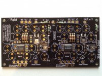
Hi Stijn,
These are the exact positions I will use for the shunts. I will only use a film cap at the pins of the dac for the analog side. I will draw Vdd supply from the B+ on the dac board, in that way I can use the digital supply for the motherboard and dac boards with minor modifications.
The two 10r resistors at the b+ entrance will be relayed with a wire to the soldering pads of the 3.3v regulator.
Than I will use one of the 4 cap positions in the row to enter the raw supply of the analog stages.
I do not recommend to put the shunts under the dac board, they get pretty hot, particularly the 3,3v, it has got a bit to high raw supply in the original setup. It would be better to feed with 6-7v instead of 12v.
Regards,
and I have no way to draw these clearly but I will give an explanation of my thinking which I think is similar to SUPERSURFER's.
Simply (?) two raw supplies - using TENT's guidelines he says 7 to 10 volts input voltage to the 3.3 volts regulators. I will use a resistor input (10R ?) after the rectifiers with around 3K uF cap to ground followed by a choke (.3 H, 11 ohms) another 3K uF of capacitance then likely an RC filter ( 10R and maybe 4500 uF capacitance) with a 7 volts transformer and a full wave rectifier the DUNCAN tool predicts just over 8 volts - the low end of Tent's recommendation but should be plenty. The leads from this supply connected directly to the 3.3 volts regs mounted per SUPERSURFER to the bypass cap "hole" that connects to the Vdd input of the DAC (I need to look at the board to tell you which is the one).
The positive lead from the 3.3 volts raw supply to the input of the reg - the output of the reg to the above mentioned hole in the PCB - the negative lead from the raw supply to the ground leg of the regulator AND to the ground point on the side of the board.
The more I think about this I thought one could get by without PCB surgery but I realize now the the +power trace must be cut. I have read Tent be of two minds about an input cap to the regulator. In the application notes he recommends 10 uF but I think earlier in the thread someone said he said none was needed. That would be preferred. If one elects to use an input cap this could be placed on the DAC board just be sure you cut the trace before that capacitor. OR you could have the cap attached to the input wiring to the reg and it would float above the board. I tend to think it is better to have the cap float.
I would retain the caps and resistors for the 8 volts supply on the board. There are three places where power enters the Vcc part of the board so one cannot be quite as elegant with the regulators input. The more I look at it one is stuck with having more path length that one would want, ideally, for the regulator. One can use any one of the three bypass cap "holes" for the regulator output but will need to run a wire to the other two and with these two it would be a good idea to use the bypass caps. One should be able to get away without the bypass cap at the input one uses for the regulator output. Again, I need to take a look at the board to tell you which one I will use. I know it will be the one that goes to pin 23 of the DAC. I am writing at work and do not have the board in front of me.
For the raw supply, extrapolating from Tent's recommendations one should use between 11.5 to 19 volts for the 8 volts regulator. Using a 12.6 volts transformer I would make it very similar to the other supply - but I would not use the last filter within the raw supply but use the filter on the board for this part of the supply. Bypass R1 - use 10R at R2. Bypass the inductors with lengths of wire and the 8 volts regulator - easily done when it is removed - just solder a wire across the two small pads. This will give you approx 15 volts at the input of the regulator.
I will attempt some kind of drawing. I know this sounds far more complicated than it really is.
This way the raw supply for the 8 volts reg will enter at the VB+ pin and ground would be attached at the ground point along with the ground wire from the 3.3 volts raw supply and from this same point the 3.3 volt raw supply ground. Daisy chained from here will the the wire to attach the 3.3 volts regulator ground pin.
First draft. I hope it makes some sense. I (and I hope others) will fill in blanks in time.
Thanks for spending the time to write this up. I agree a diagram will help as they say a picture speaks a 1000 words.
I do not recommend to put the shunts under the dac board, they get pretty hot, particularly the 3,3v, it has got a bit to high raw supply in the original setup. It would be better to feed with 6-7v instead of 12v.
Regards,
Hi supersurfer,
This was my main concern thinking to install the shunt between the two boards but I prefer to ask before to who already have experiences with this shunts.
Thanks to point it out.
Regards,
Enrico
Hi Stijn,
These are the exact positions I will use for the shunts. I will only use a film cap at the pins of the dac for the analog side. I will draw Vdd supply from the B+ on the dac board, in that way I can use the digital supply for the motherboard and dac boards with minor modifications.
The two 10r resistors at the b+ entrance will be relayed with a wire to the soldering pads of the 3.3v regulator.
Than I will use one of the 4 cap positions in the row to enter the raw supply of the analog stages.
I do not recommend to put the shunts under the dac board, they get pretty hot, particularly the 3,3v, it has got a bit to high raw supply in the original setup. It would be better to feed with 6-7v instead of 12v.
Regards,
Stefan, It had probably occured to you already as well. Looking at the layout, the the outer side hole for R1/R3 which you are planning to omit, (hole nearest to the caps) will lend itself well for a vertical wire to create a common power point for the Vcc feed.
I'm currious what you are planning for a grounding scheme, as I suspect you'll need a star ground somewhere to keep the seperate powersupplies in check.
An externally hosted image should be here but it was not working when we last tested it.
In an attempt to understand what Rick and Supersurfer are discussing, I drew up this picture. Is this what is being proposed?
Any comments?
I think you can remove 2 more of the electrolytics. The lowest 2 can stay, but the 2 above those shouldn't be needed as I understand.
Do you mean a wire jumper across the in+out pads for the original regulator? Surely that will put full v+ direct to the DAC. Removing the caps won't break the circuit as they're all for decoupling.When using the regs this way it is simple enough to place a wire across the small pads of the removed original regulators completing the circuit.
These are easy to remove for those who have not yet attempted. Just be patient.
Also, maybe I lack patience, but I certainly didn't find it easy removing the old regs from the board, but my board was already fully populated at that point. Removing them from a bare board would be much easier.
Hi,
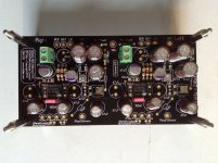
Attached is the layout I will build, shunts not mounted because they are still running in my other dac.
The two holes of R1 and R3 are a good spot to connect the B+ through to the other boards.
You need to cut the traces going to the pin of c28/30 and mount the output of the shunt on this spot. In this way you can solder in some local oscon upstream of the digital shunts.
The green connecters are for putting in analog power, no need to connect ground if you have the grounds from digital and analog connected in the raw power supply.
I will use three silmics of 100uf and after the 10r resistor 47uf; these different values will make a nicer sound balance.
The three wimas on the analog dac pins are needed but I want to experiment with different types because they have a clearly audible effect and need to be tuned for best sound balance.
I am now still waiting for the last parts to arrive (and will be at Pinkpop this weekend) so no soldering this weekend
Regards,
Attachments
Hi James,
I will stick with the 16 shunts as it is the best option. If you are on a budget you can try to use them for more boards prallel but I guess you can use them on not more than two boards because the current draw will be to high. The shunts are also adjusted to the drawing current by Tentlabs. You need to consult them to check the max. Current draw.
Regards,
Last edited:
Elegant input scheme for 8 volts regulator
I could not decide how to handle that and I cannot think of anything better than your approach.
I assume you will bring raw supply for 3.3 v reg to the output pad of the removed regulator?
That seems like a rather large wire you are using. Is it something you have found to be really good?
With my mock up in progress I find I run out of space quickly. I will have to mount the regs on the front and the back of the PCB.
Take care,
Another picture where you can see the wire bridges more clearly
I could not decide how to handle that and I cannot think of anything better than your approach.
I assume you will bring raw supply for 3.3 v reg to the output pad of the removed regulator?
That seems like a rather large wire you are using. Is it something you have found to be really good?
With my mock up in progress I find I run out of space quickly. I will have to mount the regs on the front and the back of the PCB.
Take care,
Thanks to all of you guys for making this mod so clear with the sharing of diagrams, pictures etc.
I'm waiting for when I get the chance to dedicate some time to my 2 deck build with 4x sjostrom super regulators. I feel that it will offer the same performance as the shunts if not better, with a current capacity that would easily extend to 4 decks, if not 8.
Removal of the surface mounted local regulators on an unbuilt board is quite straightforward and I understand that it would be complicated to offer PCBs both with and without those however, I would like to support the idea of having the PCBs available without bundled components as, like Stefan, would prefer to choose my own passive components.
- Home
- Source & Line
- Digital Line Level
- A NOS 192/24 DAC with the PCM1794 (and WaveIO USB input)