I assume you will bring raw supply for 3.3 v reg to the output pad of the removed regulator?
That seems like a rather large wire you are using. Is it something you have found to be really good?
,
Hi Rick,
This mod will bring the raw digital supply from the B+ rail to the output pad of the 3.3v regulator.
The large wire is not important; there is extra buffering with oscons behind the wire, so the shunt will effectively see the low impedance of the oscons.
Regards,
Hi,
Attached is the layout I will build, shunts not mounted because they are still running in my other dac.
The two holes of R1 and R3 are a good spot to connect the B+ through to the other boards.
You need to cut the traces going to the pin of c28/30 and mount the output of the shunt on this spot. In this way you can solder in some local oscon upstream of the digital shunts.
The green connecters are for putting in analog power, no need to connect ground if you have the grounds from digital and analog connected in the raw power supply.
I will use three silmics of 100uf and after the 10r resistor 47uf; these different values will make a nicer sound balance.
The three wimas on the analog dac pins are needed but I want to experiment with different types because they have a clearly audible effect and need to be tuned for best sound balance.
I am now still waiting for the last parts to arrive (and will be at Pinkpop this weekend) so no soldering this weekend
Regards,
Thanks for the picture. Very clever to cut the trace downstream from C28/C30 and to connect ground of the 3V Shunt at the powersupply. That should prevent the risk of groundloops significantly.
Would there be a benefit in using position C2/C7 instead of C4/C10 to keep grounds completely seperated between the 3V and 8V feeds?
Hi Thommy,
Are these shunt or series regulators?
Neither, they are super regulators as in the work of Walt Jung. LM317 based.
Attachments
Last edited:
Caps C21 and C22, C24 and C25
Which are connected to the 2 Vcom pins and after the regulator - one wonders if these could be a problem for the shunt regulators? Seems they have to be there. Do they need to be 47uF? The TI spec sheet uses this value in their "typical connection diagram".
But this comment from Tent gives one a little concern:
I recommend not to have capacitors behind the shunts so better leave them out. This is only possible if the shunts are close to the chips. If they are more than few cm away, than a small nice film cap close to the DAC chip is fine.
I know some have already installed these and obviously have not had problems but one wonders if it would be better to use a (much?) smaller capacitor than the 47 specified? I have looked around and find nothing that says anything about the acceptable range.
Any thoughts on this?

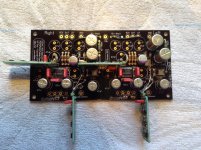
Guess what the mail man brought yesterday?
The new dac boards are playing!
Here is a picture of the way the dac board is build up.
Will post more next week, need to go to my listening chair now.................
Looks great! Curious what your first impressions are.
Thanks for the picture. Very clever to cut the trace downstream from C28/C30 and to connect ground of the 3V Shunt at the powersupply. That should prevent the risk of groundloops significantly.
Would there be a benefit in using position C2/C7 instead of C4/C10 to keep grounds completely seperated between the 3V and 8V feeds?
There are two ground planes; left and right, digital and analog are share the same ground.
After seeing all theses mods I wonder if it would not be better to just redesign the boards all smt affairs, much smaller in size and with all the components we don't plan to use left out? Doede maybe you can sell either fully populated or completely empty all smt boards?
This would get rid of empty component locations, unused vias, jumper wires and tall things acting as rf antennas, completely separate power supplies for analog/digital and maybe even left/right channels and keep the ground planes for digital and analog separated.
From this Analog Devices article: Staying Well Grounded :
Nevertheless, if a high-accuracy mixed-signal system is to deliver full performance, it is essential to have separate analog and digital grounds and separate power supplies.
Thanks Stefen for keeping us all up to speed!Guess what the mail man brought yesterday?
The new dac boards are playing!
Here is a picture of the way the dac board is build up.
Will post more next week, need to go to my listening chair now.................
")
Pls keep us posted with ya findings on this recent mod...! So eager to desolder my DAC and....!
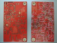
new board
Hello to you all,
Sure Palmito you are absolutely right.
You are paying for a stuffed board, the you need to '' abort '' most of the parts to do some improvements. YES you neede to do them because it will be a giant step forward and you will end up with something that sounds very nice but looks like a messed up prototype.
I am sure there is a big group of diy people who will decide not to go for this dac because they dont wanna have this kind of circuit board once they are ready.
Maybe the next production run have another board available that is meant to be upgraded and will have a very decent look when it is done.
Almost sure it can be done in such a way that it will even be an improvement compared to all the tricky things done so far. If the board adjustment is done in a proper way it will easier to put some more boards on top.
But having some nice chokes in stock it probably would be easier to upgrade the power supply first. Anyone did try choke input?
Sincere greetings, edward
I have been following this recent modification from Supersurfer with great interest! Myself have already got 8-decks up and running with Doede PS. Yesterday, I was able to have real listening experience to Stefan replica raw PS design at a friend. While this replica is none optimised, I was so flatter to learn how good it was and dare not imagining how better it can be with better grade diode(s), transformer, chokes..., and caps! After listening, I went home and done some damages to my bank account with these Chokes based on a friend recommendation.
Here is a preliminary trail replica 'Stefan's raw PS' at a friend place.
An externally hosted image should be here but it was not working when we last tested it.
Here is a preliminary trail replica 'Stefan's raw PS' at a friend place.
An externally hosted image should be here but it was not working when we last tested it.
Hello,
I remember reading in a French audiophile magazine long time ago that one should use conventional ( EI type) transformers for digital gear because they will stop all kind of parasitic noise from your digital filter going back into your mains.
Do some reading on choke input because they have a high current rating you will be able to attach a bleeder so there will always be enough current running making the system work like a true choke input.
Good luck, Edward
Nice one, thanks for sharingGuess what the mail man brought yesterday?
The new dac boards are playing!
Here is a picture of the way the dac board is build up.
Will post more next week, need to go to my listening chair now.................
That all makes good sense when I see it like that.
Looks like a good plan, certainly nobody's going to get the Digital regulator closer to the DAC chip than that!
Does the trace to C28/C30 which needs cutting run on the underside of the board?
Is there a reason you didn't use the Rload common to ground the analog regulator? Is it just because it would make the construction of a multi-deck version more difficult?
thanks again,
James
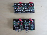
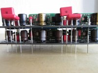
Because this is the first time I am using shunt regs for a DAC and I wasn't sure how important the placement of the shunts really is I did a test now.
I have 4 DAC boards and because I use pcb connectors between the boards it's easy for me to switch between different modifications.
On the first board the output of the 8V shunt reg is soldered to the pads of C18/C20 and the 3.3V shunt to C14/C16. On the second board 8V to C17/C19 and 3.3V to C28/C30. So on the second board the 3.3V shunt reg is 1.5 cm closer to the DAC.
The difference is clearly audible and bigger than I expected. The second board sounds more "direct" and "airy". The separations of instruments is better. Both boards sound good, but if I switch from the first board to the second board everything seems to be more in place and listening more relaxed.
So placing the regs directly at the DAC with no caps seems to be a better solution than the regs at bigger distance and a cap close at the DAC.
In another test I compared a board with Silmic caps to a board with the original Muse caps. I expected the Silmic to be better, but in summary I like the Muses better. The Silmic have better mids, so voices sound nicer and more pronounced. But to me they also sound a bit to soft. The Muse caps give a more kicking bass and more details. Maybe just a matter of taste. Think next I will also test some Panasonic FC and maybe a mix of different caps on one board.
Regards,
Attachments
very cool, thanks for sharingBecause this is the first time I am using shunt regs for a DAC and I wasn't sure how important the placement of the shunts really is I did a test now.
Do you have a part number for those stacking pcb connectors?
Just to add, I think the placement of the 3.3v digital regulator, the same as Stefan did is perfect. As close as it can be, but if the close placement is so critical, then the second placement of the 8v analogue shunt is only a really close for 1 of the DAC channels and not the other because of the way the board is layed out. Because it's running in Dual Mono and both the channels from each DAC chip get merged anyway, I don't know how much of an issue it makes though.Because this is the first time I am using shunt regs for a DAC and I wasn't sure how important the placement of the shunts really is I did a test now.
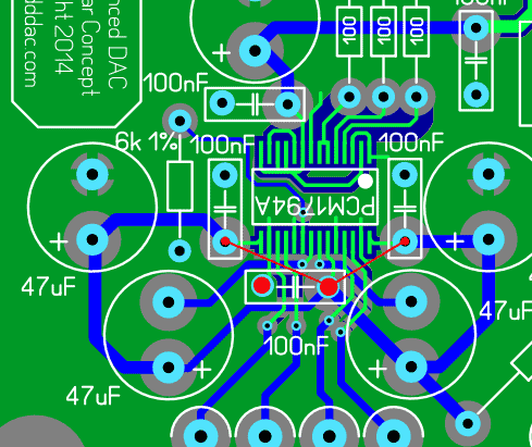
Here's the updated board layout I got from Doede so you can see all the traces:
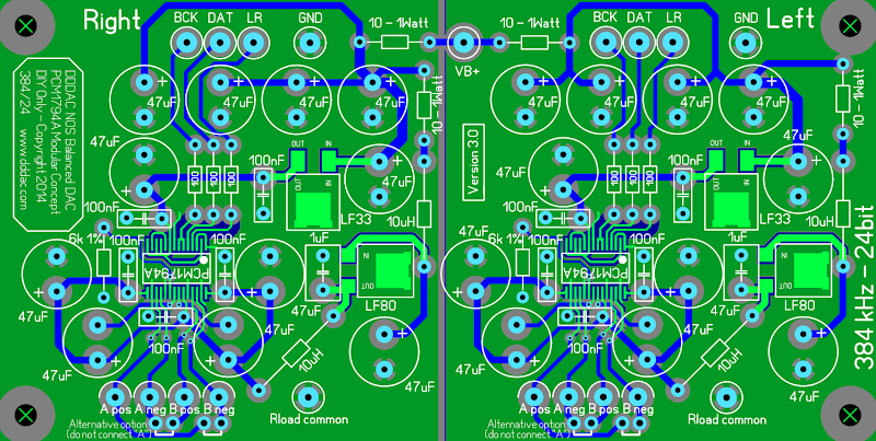
and here's the pinouts of the chip from the datasheet:
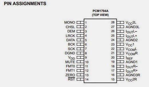

It seems to me if you wanted to have the 8v Analog regulator as close as physically possible to all 3 VCC DAC pins, the best way would be to run them in the C23/C26 position and maybe run short wires underneath the board to C17/C19 and C31/C33. I can't see another way to have a shorter path. Would it make an audible difference though? Something like this:
BTW, is it easy for you to test how much difference it makes just moving the Digital 3.3v regulator?
very cool, thanks for sharing
Do you have a part number for those stacking pcb connectors?
Hi james,
I got them from a local store here in Berlin: SEGOR-electronics GmbH, Berlin
They are normal pinheaders only a bit longer, so that I still can stack the boards above each other.
The pins are still a bit short. OK for testing but probably not for longtime usage. On the picture they don't look straight, but thats a fault of the camera.
Attachments
Yes I know that, think also Rick McInnis suggested that. It's also on my list for testing. But because of the caps it's not easy to place the shunts there.It seems to me if you wanted to have the 8v Analog regulator as close as physically possible to all 3 VCC DAC pins, the best way would be to run them in the C23/C26 position and maybe run short wires underneath the board to C17/C19 and C31/C33. I can't see another way to have a shorter path.
Sorry, I have no board with the 8V shunts soldered to the pads of the LF80. They have been from the beginning with the output at the pads of C18/C20.BTW, is it easy for you to test how much difference it makes just moving the Digital 3.3v regulator?
- Home
- Source & Line
- Digital Line Level
- A NOS 192/24 DAC with the PCM1794 (and WaveIO USB input)