You can get the impedance to a more sane level in a 2 layer by closely edge coupling the lines to surrounding ground planes, as well as the rather too far removed ground plane of the reverse of the board, this needs fairly careful layout.
These days I personally tend to 4 layers as a minimum for anything involving digital parts, a buried ground plane under a thin prepreg makes that side of the board very convinient for sane impedances, and edge rates (and package densities) are IMHO just too high to make doing without a ground plane worth the pain.
Fact is that these signals are RF, and good RF design practise really benefits from ground planes and microstrip or stripline designs, both of which work much better with a plane or two much closer then common 2 layer supports.
Two layer is fine for audio, but converters are fast mixed signal and for that, two layer is very, very marginal, the really fast stuff really needs 8 layers which gives you 4 routing layers and 4 planes.
50 Ohm single ended, or 100 ohm differential works for me (and allows standard cabling), source terminated with load terminations only if using proper line recevers that can cope with matched impedance as opposed to voltage transfer.
Regards, Dan.
haha lots of activity here since the browser crashed with my reply, soz I didnt nor do I have the energy to do all of it again, but yeah basically I started thinking about it and though both are following consistent characteristic impedance between their own boards, ackos are rogers teflon and Ians are fr4, so even though both follow the same spec and same foil weight and follow transmission line construction, they cant really be totally matched I wouldnt think? Ackos match Ackos and Ians match Ians, I dont know enough detail about the spec to talk about it, but I know the modules within the systems are consistent and then they both use w.fl and u.fl. so no probably not perfect
but better than a ribbon cable and connector IMO, better than opinion, in my experience, I get more consistent locks at lower DPLL settings and higher speeds than with ribbon.
havent seen 4 layer for audio? really? buffalo II is 4 layer afaik, the wire and all of opcs boards except maybe NTD1 are 3 layer (4 layer but one layer completely deleted as wasnt needed) also the regulator, battery monitor, MCU, digital volume and digital input PCB I got made for my transportable dac/headphone amp is 4 layer
a standard would be awesome!! fat chance. youve got as much chance of that as a standard balanced headphone connector being decided on...
Last edited:
You can make it lower, which may or may not be better for what you're trying to do. Nominally it's a decent way to get to 100 ohms on two layers---if one's working 0.5mm pitch with the usual SGSGSGSG connector pin assignment in 7 mil DRCs that's a 7 mil trace with 13 mil gaps and 20 mil ground traces. The problems are with stapling vias on the ground trace---usually those are 25 mil pad---and fan out from chips with SSSS pinouts. Given most audio designs aren't that dense or fast neither issue is a particularly big deal.You can get the impedance to a more sane level in a 2 layer by closely edge coupling the lines to surrounding ground planes, as well as the rather too far removed ground plane of the reverse of the board, this needs fairly careful layout.
Perhaps. Every reference design and eval board I've looked at is two layer, including the ones for flagship DACs and mixed signal DSP implementations. The headline performance figures in the datasheets are measured on the same boards so, if there's performance gain to be had from more than two layers, there'd be a very strong financial incentive for manufacturers to up the layer count in their eval boards. So it's kind of interesting that they haven't, even for sensitive mixed signal parts like multi-GHz jitter cleaners.Two layer is fine for audio, but converters are fast mixed signal and for that, two layer is very, very marginal, the really fast stuff really needs 8 layers which gives you 4 routing layers and 4 planes.
A definitive answer requires building and measuring any given design with 2, 4, n layers but---given one can hit jitter of a few hundred fs, noise floors of a couple hundred nV, and nonlinear distortions of a uV or two in two layer---increasing layer count is unlikely to improve performance that much. In my experience the main advantage of 4+ layers is you work a lot less hard to get a good layout and (if building a commercial product) pass emissions requirements.
They can, it just requires a wider trace on acko's boards to compensate for the lower dielectric constant (assuming equal thickness). How much narrower depends on which Rogers materials and which FR4 types are in use but it's probably within roughly factor of two. 7 versus 15 mils isn't the end of the world but it can be a showstopper with wider traces.ackos are rogers teflon and Ians are fr4, so even though both follow the same spec and same foil weight and follow transmission line construction, they cant really be totally matched I wouldnt think?
For most applications Rogers and u/w.fl are overkill so I would tend to bet the improvment in lock rates is more about the overall quality of the system engineering and integration than the choice of parts, particularly given ESS's very low DPLL bandwidths. Would be interesting to measure the signals but that goes back to our earlier conversation about cost of required measurement gear > DIYer budget.
Hmm, yeah, I forget too---but it probably is since Twisted Pear's website calls out the B3 as four layer. Not familiar with OPCS; got a link?buffalo II is 4 layer afaik
Especially if one starts with the premise it's not going to happen.a standard would be awesome!! fat chance. youve got as much chance of that as a standard balanced headphone connector being decided on...
") I think one can choose two values that easily satisfy most requirements---50 ohms and something in the 90-140 ohm range, with 100 ohms probably being the most compelling candidate---and eventually avoid most of the fuss as adoption builds over time. One would still need to convert between 50 and 100ish sometimes but the key to making that a solvable problem is simply standardizing the two values between which conversion is required. If folks can agree on a value suitable for two layers I'll lay out the expansion connector on my DSP+DAC board in compliance with it.
I think one can choose two values that easily satisfy most requirements---50 ohms and something in the 90-140 ohm range, with 100 ohms probably being the most compelling candidate---and eventually avoid most of the fuss as adoption builds over time. One would still need to convert between 50 and 100ish sometimes but the key to making that a solvable problem is simply standardizing the two values between which conversion is required. If folks can agree on a value suitable for two layers I'll lay out the expansion connector on my DSP+DAC board in compliance with it.The TI evaluation module for the PCM5102 has four layers on the digital side and two layers on the analog side of the board. They must have found a reason for doing that. They talk about it somewhere in the description.
http://www.ti.com/lit/ug/sbau190a/sbau190a.pdf
http://www.ti.com/lit/ug/sbau190a/sbau190a.pdf
Interesting. It's even in the silkscreen on the board (see figure 1). Unfortunately only the top layer is shown in the doc so it's hard to tell what would drive the need for four digital layers and the choice to use only two "analog" layers.TI said:It should also be noted that the digital interface section, or left half of the PCM510xEVM-U, is a four-layer design. However, the PCM510x device and analog circuitry, or right half of the EVM board, consists only of two layers.
This is digital part of audio, and for any digital 4 or more layers is better, as you realy need at least one contigous ground plane. The comercial designs tend to use a multi layer for the digital interface, and over tha past several years many of them have used this fact as a bullet point in there advertising.
Yes DIY is simpler using two layers, but if you want the ultimate signal integrity for your digital section then 4 layers plus is the way to go. There are multi layer projects on this site in the digital section.
For the DIYer it is getting easier and cheaper to do 4 layer boards, there is now free PCB software that will do mullti layer, and the cost of having 4 layer boards is dropping, with some good deals from manufacturers, but not for one of quantitries, which is a shame.
I'll see if the texas site has gerbers or PDFs of the layers they often do. What gets me is how the board dosn't warp, we get whinged at by manufacturers if all out layers are not balanced for copper. Also I have numerous app notes and analogue news letters etc from texas where the discuss analogue/digital board and how to seperate the signals and handle one contigous ground plane.
I suspect in this case trhey are aware that the analogue end may get modified and it does make things easier to mod and play with on 2 layers.
The nearest I have done is a multilayer with 4oz copper on one half and 2oz copper on the other half, multilayer, but it was a thick board, and bolted down to an 8mm case wall.
PCM51xx gerbers and PDFs available at the bottom of the page.
PCM5100 Evaluation Module - PCM5100EVM-U - TI Tool Folder
PCM5100 Evaluation Module - PCM5100EVM-U - TI Tool Folder
Since we're on this slight tangent of diy designs with more than 2 layers I thought I'd put together a list of ones that I could think of off the top of my head.
opc has a series of 'The Wire' Projects:
headphone amplifiers 3 layer boards for amplifier and bipolar regulator - the first link should take you to a photo of the test setup and the detailed measurements are in the posts directly before that. There is a wiki page with build guide and schematics here
LPUHP
LME49830 Class AB Amplifier
Per-Anders Sjostrom also has some very nice designs documented on his website and pcbs available for most of them. This includes even a 4 layer rectifier + snubber pcb; his 4 layer layout of a modified Jung super regulator; some headphone amplifiers and diamond buffer designs, and more ...
Anthony Holton of Aussie Amplifiers has a few pcb layouts that appear to be more than just the run of the mill two layer design, though I can only find reference to his DAC layout being 4 layer.
Moving to more digital side of diy audio we have:
TPA BIII - 4 layer
WaveIO - 4 layer
Ian's I2S FIFO
ackodacs are also far from the average diyer's pcb layout
I am certain that there are more out there in these forums that I havent found.
That is the projects that I could think of off the top of my head just now. Certainly there are plenty of 2 layer designs still but I have, over the last year or so that I have been pursuing diy audio as a hobby, acquired more pcbs that are >2 layers than I have 2 layer boards and most of the 2 layer boards have been used in experiments only then left behind for various reasons.
And there'll be more of them as PCB prices gradually continue to drop. Thanks for the data points; obviously more kit/DIY/DIY vendor adoption already than I was guessing---four layer is ~USD 1/sq. inch for a 100 board run so the economics are fairly tractible if one's got a board that'll sell.I am certain that there are more out there in these forums that I havent found.
Yeah, every time I've looked at BatchPCB, OSH Park, PCBFabExpress, and similar for four layers it ends up being just about or more cost effective to do a one of the small runs at Gold Phoenix. The BOMs for my projects are ususally in the $60-130 range per board, which means a four layer PCB ends up costing as much or more as everything else combined. The designs are simple enough I can usually get pretty close to a continuous plane on the back of the board so paying 3.3x the two layer board cost to have four layers has yet to be compelling. But I like layout and enjoy working the design to find elegant solutions; if I was billing hours four layer would be cheaper every time.the cost of having 4 layer boards is dropping, with some good deals from manufacturers, but not for one off quantities
Thanks. It's a little off topic but any recommendations for a gerber viewer? I don't actually have one installed.PCM51xx gerbers available at the bottom of the page.
GC prevue, its free.
GraphiCode - Software Innovations for Electronics Manufacturing - Gc prevue
GraphiCode - Software Innovations for Electronics Manufacturing - Gc prevue
slightly off topic but not irrelevant - whilst attempting to install my ribbon cable I note some differences on the pcb boards:
USB->I2S
6 pcb holes
MCLK, LRCK, DATA, SCLK, GND, 5V
I2S->DAC
5 pcb holes
DATA, GND, WS, GND, BCK
Is anyone able to clarify which connections are required?
USB->I2S
6 pcb holes
MCLK, LRCK, DATA, SCLK, GND, 5V
I2S->DAC
5 pcb holes
DATA, GND, WS, GND, BCK
Is anyone able to clarify which connections are required?
Last edited:
you dont need MCLK thats not officially part of i2s format, some use ity, but not yours
Data = Data
LRCK = WS
SCLK = BCK
try to connect a ground in between each signal so connect
GND->GND
Data= Data
GND = GND
LRCK = WS
GND=GND
SCLK = BCK
GND = GND
you can skip the last GND if you like
Data = Data
LRCK = WS
SCLK = BCK
try to connect a ground in between each signal so connect
GND->GND
Data= Data
GND = GND
LRCK = WS
GND=GND
SCLK = BCK
GND = GND
you can skip the last GND if you like
Last edited:
Good discussion.
Firstly, I don't quite get how the grounds fit in to this.. Are they just unconnected at the destination/sink end? like http://i.imgur.com/lOykPOy.png
or should they connect the signal pin on the receiving IC to the ground plane on the source chip's PCB? or what?
Secondly, how best to connect a ribbon connector to the source board (2 layer with ground plane)..
Is it best to place the ribbon connector on the top, leaving the signal lines on the same layer, and then place a small ground zone on the top side to connect the grounds to ('A' in http://i.imgur.com/vAfqrJm.png), or like A but just with vias to ground plane (no top ground zone).. or place the connector on the rear and connect route the signal lines top the top through vias (B in image). Putting the connector on the top is preferred if it doesn't make much difference, though.
If there should be a front ground zone; are there any guidelines on how best to connect it and the rear ground plane? (eg. no/ positon of vias) Does the size matter at all?
[image legend: green=rear gnd plane, red=front gnd zone, blue=ribbon connector, yellow=via]
Thirdly, the MCLK. I take it that it is the fastest signal and therefore most problematic.. so what is the benefit of using it, if it is optional? If it is unused should it just be left unconnected on the IC. Or should it always be used if available?
FWIW i'm looking at TI ICs for both source/sink, which both offer MCLK connectors.
[edit:] Also, if resistors are used at the source end (which I understand is wise), should effort be made to place them as close to the source IC as possible, or is anywhere before the ribbon connector fine?
Thanks.
Last edited:
Hi,
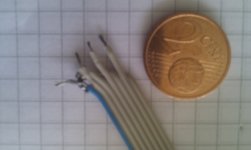
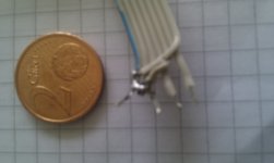
Is this DIY cable good enough for 8 to 10 cm of I2S ?
Its GSGSGSG : 7 cable which 4 Gnd soldered together but the 3 gnd cables recover the 3 hot cables with 90° to be sold together on the fourth gnd (blue one).
What is the worst here ? Bad diy like that with this length or stay SPIDF with 20 cm but full 75 ohms ?
On one side we have the Squeezebox Duet Xilinq chip with 3 x 25 ohms resistor and of the other side I2S line for ES9023 with the possibility to have 50 ohms resistors (Subbu DAC). If I2S better than SPIDF here, do I supress one of the two grups of serie caps (the 25 ohms on the emiter, we keep it always at the end ? or reverse reflexions can occur also towards the emitter?
Series: 25 ohms 5xilinq chip) + 8/10 cm bad cable + 50 ohms = around 75 ohms !
thanks
Attachments
- Status
- This old topic is closed. If you want to reopen this topic, contact a moderator using the "Report Post" button.
- Home
- Source & Line
- Digital Line Level
- i2s cable/wire type