https://www.mouser.com/PCN/Integrated_Silicon_Solution_Inc_EOL_39LV512_49FL004T_20170515.pdf
It EOL. I need something that's in production.
It EOL. I need something that's in production.
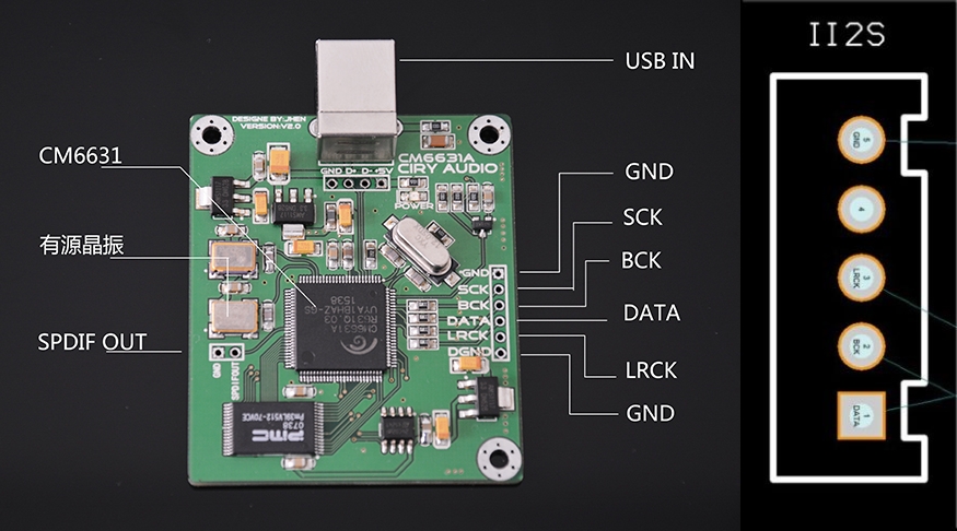
Hey there. I have the same board pictured here, with CM6331A-
I use it with a laptop currently, and it works fine.
Is it compatible with Android based tablets? I have a Samsung Galaxy Tab 4 and a Google Nexus 10 that I would like to use primarily as media tablets, and was wondering if additional software or chicanery was required.
I use it with a laptop currently, and it works fine.
Is it compatible with Android based tablets? I have a Samsung Galaxy Tab 4 and a Google Nexus 10 that I would like to use primarily as media tablets, and was wondering if additional software or chicanery was required.
Hi expert just a question for my noob knowledge at DAC. in the CM6631A datasheet its written : Connects to an external parallel Flash/EEPROM memory (Max. 64KB, 55ns access time is required) for firmware codes i search for a lot of pics in the net with cm6631A boards and all PM39LV512 are with 70nsec...so its is ok? can somebody explain me thisBoth CM6631A and PM39LV512 difficult or impossible to get a hold of through official channels. Are these parts at the end? I really don't want to touch XMOS and the programming required.
chris
Hey there. I have the same board pictured here, with CM6331A-
It should work with an OTG cable if the firmware is standard.
This may seem like a silly question but with regards to the parallel flash is there any reason why you actually need to connect D0-7 and A0-15, on the CM663x, to the corresponding number on the flash chip itself?
In other words D0 to D0, D1 to D1.
I can't think of any exact reason why you need to do this.
For example lets say you were to connect A0 to A15, A1 to A14 etc and have the pins going backwards.
Under normal circumstances you'd have them A0 to A0. So lets say you want to write 0xFF into address 1. A15 to A1 would all be held low and A0 high on the CM663x and you'd end up with 0xFF stored at address 1 of the flash memory. The CM663x would think 0xFF is stored at address 1, so to recall that data it would hold A15 to A1 low and send A0 high, then perform a read, it would then get FF.
But if A15 to A0 are reversed at the flash chip, the CM663x would still hold A15 to A1 low and A0 high to store at address 1. This time though the flash chip would have A15 held high and the rest low as the pins were reversed. The CM663x would write 0xFF and it would be stored at 0b1000000000000000. To recall this data the CM663x would send out a 1 on the address pins, but the flash would see a 0b1000000000000000 and the CM663x would still get its 0xFF.
Everyone seems to route A0 to A15, D0 to D7 then have a struggle routing all the traces. But surely you just can connect the address and data pins of the CM663x to any order of address and data pins on the flash memory and everything would still work. Sure that would make everything only compatible with your PCB but that's not really a problem when you're only DIYing a couple of boards.
Am I missing something?
I could see this being a problem if sequential or bulk data transfers happened (like with serial interfaces), but do they happen with parallel storage, apart from a bulk erase?
There is always some hardware protocol for talking to Flash/EEPROM. Access time is only one requirement, the replacement part you use would have to operate in exactly same way the old memory chip did (in terms of addressing modes, read/write control, etc.), otherwise the CM6631A would not know how to talk to it. Maybe CM6631A firmware could be modified, or maybe the memory chip requirements are defined in hardware and un-changeable. Don't know if anyone here has looked into it deeply enough, but it doesn't look good seems to be general consensus. If you want to buy the old memory parts from a distributor that specializes in stocking discontinued parts, you might be able to find the old, original part there, at least until stocks run out.
Parallel flash is very basic as everything is handled via hardware pin commands except bulk erases.
Bulk erases are necessary and are performed prior to the programming of data.
When you bulk erase you set all bits of the memory to 1. When writing data you cannot toggle a 0 to a 1, you can only set a 1 by a bulk erase. So prior to writing data, you have to erase everything to ensure that what you want to store gets stored correctly.
Bulk erases occur by writing certain commands into the chip and if you altered the pin orders you'd mess this up. So A0 has to go to A0.
These erase commands are common across chips of the same series/type so you can interchange flash from one company with flash from another.
Also the sizes of the flash memory aren't important either. Bigger chips (than 512k) are common these days and they come with additional address pins. The CM chips only have A0-A15, but these chips come with A16, A17 & A18. As we don't need to access these memory locations, for either bulk erases or for writing to/reading from, you can just tie them to ground and leave them unaccessed.
The only caveat is the bulk commands for one set of chips and another seem to vary ever so slightly.
Some use a command address 12 bits long and others use 16 bits.
Ie some send 555h and some send 5555h.
I am looking into this.
If you search the internet for CM6631A you'll find the common memory used is the PM39LV512-70 from PMC. These use 555h/12 bit addressing.
DIYinHK, however, use a 39VF010-70 chip from SST. This uses 5555h/16 bit addressing and is 1M in size so it's something that can be worked around.
Many many companies also use 70ns chips. The ones above are 70ns, ASUS uses 70ns too, so clearly that's not a concern.
If you look at the schematics provided by tdtsai, the memory chip is classed as a SST39lf010-45-4c-whe. Although obsolete the datasheet says that it uses 5555h/16 bit address, so maybe it doesn't matter. Perhaps the 4 MSBs are ignored with the devices that use 12 bit addressing for commands so the 12 and 16 bit parts are interchangeable.
The 555h/5555h is the biggest issue. I'm going to look through the firmware programming stuff to see if there's anything that mentions the flash programming. It's possible that side of things is baked into the compiler thingy that tdtsai has provided and you cannot change it. It'd be nice if he chimed in!
It took some more time to come up with a new version. The reason is that I had to add a CPLD mainly due to the need of a direct/drc switch and that the firmware of the CM6631A using the XMADC input interface uses 24bit left justified data and is master (my conclusion after reading documentation back and forth a few times). The design would have been more clear if it was a I2S slave interface. But as I dont want to go into firmware changes, I could not see another solution. Just hope it works.. Comment are more than wellcome
By the way, I'll keep the ESD diodes on the USB lines for extra protection. Impedance matching = yes I will do.
/Anders
I don't know if you have built this yet, I find the datasheet and the schematics provided by tdtsai somewhat confusing at times.
Referring to your schematic XPWDN is an output for toggling external codecs yet it looks like you've connected it to a pull up resistor.
The datasheet mentions two different ways of powering the chip, self power or bus power. Nothing is detailed about what this actually means but you've got XSEL_PWR held high, indicating self power. I am assuming that this means the chip gets its power from an external 3.3v source rather than the USB bus. Do you know exactly what happens if you do go with bus power? What exactly do you have to change with regards to the hardware configuration and voltage regulators with bus power?
Speaking of power, Vcc is apparently the output of a 2.5V internally regulated rail and is where you're supposed to connect external decoupling. You have it tied to the 3.3V rail though.
Okay so update. I got something working just as a proof of concept.
My first board had no flash memory, I was trying to see if you could configure the thing over I2C. You cannot. Go figure. It would be too easy if you could do that, disable the device, update register settings via a ucontroller, enable and boom working. No we have to use this convoluted firmware. Of course that might be easier for some. Unless I am oversimplifying what the onboard ucon of the CM663x actually does.
The second one was done using flash memory, which should be foolproof but ya know the flash memory was obsolete yada yada. So again things needed testing.
Here's the preliminary board built up for proof of concept.

And I used a SST39VF040-70-4C-WHE memory chip.
Ignore the blue wires I got ahead of myself in the layout and botched the input > output of the 3.3V regulators by copying an old incorrect PCB layout Anyway I got it working. This is using the CM6632A as I want multichannel support and using the basic provided firmware, just to check that things work.
The cmedia firmware uploader is a pain in the ****. The damned thing doesn't work with windows 10. PLEASE fix this oversight.
I've got two older PCs with windows 7 on. One is a laptop and one is a PC. The laptop loaded the firmware uploader but couldn't see the CM6632A What a joke.
Thankfully the PC could see both and worked reasonably well. After erasing the firmware it took me a moment to figure out that I needed to unplug and replug the CM6632A before it would write new firmware successfully. It all seems a bit buggy but it got there in the end.
Both full speed and high speed operation work. Obviously full speed limits you to 96kHz for 2 channel and 48kHz for multichannel.
Switching the device into high speed mode opens up everything else up to 192kHz.
Here's a couple of screenshots.

Seems decent enough.
I haven't actually testing the thing for sound yet but the outputs do what they are supposed to. Now it's a case of getting to grips with the firmware to make the thing to exactly what I want.
The standard firmware provided for the CM6632A appears to be configured to use two ADC inputs, one for a microphone and one for a line in. Then it uses the 2 channel I2S outputs for a set of headphones and the 8 channel I2s outputs for multichannel surround sound. All work up to 24/192. And all are selectable as the default sound device.
Then you've got the SPDIF inputs and outputs too, both which will go up to 24/192. It's also possible to send the SPDIF input to the outputs to 'listen' to it using the windows configurations.
All in all there's not a whole lot that you really need to do to the settings to make the thing work, unless you want to alter the oscillator frequencies etc. It will work just as is.
In a sense this is already fully configured and
My first board had no flash memory, I was trying to see if you could configure the thing over I2C. You cannot. Go figure. It would be too easy if you could do that, disable the device, update register settings via a ucontroller, enable and boom working. No we have to use this convoluted firmware. Of course that might be easier for some. Unless I am oversimplifying what the onboard ucon of the CM663x actually does.
The second one was done using flash memory, which should be foolproof but ya know the flash memory was obsolete yada yada. So again things needed testing.
Here's the preliminary board built up for proof of concept.
And I used a SST39VF040-70-4C-WHE memory chip.
Ignore the blue wires I got ahead of myself in the layout and botched the input > output of the 3.3V regulators by copying an old incorrect PCB layout
Anyway I got it working. This is using the CM6632A as I want multichannel support and using the basic provided firmware, just to check that things work.The cmedia firmware uploader is a pain in the ****. The damned thing doesn't work with windows 10. PLEASE fix this oversight.
I've got two older PCs with windows 7 on. One is a laptop and one is a PC. The laptop loaded the firmware uploader but couldn't see the CM6632A
What a joke.Thankfully the PC could see both and worked reasonably well. After erasing the firmware it took me a moment to figure out that I needed to unplug and replug the CM6632A before it would write new firmware successfully. It all seems a bit buggy but it got there in the end.
Both full speed and high speed operation work. Obviously full speed limits you to 96kHz for 2 channel and 48kHz for multichannel.
Switching the device into high speed mode opens up everything else up to 192kHz.
Here's a couple of screenshots.
Seems decent enough.
I haven't actually testing the thing for sound yet but the outputs do what they are supposed to. Now it's a case of getting to grips with the firmware to make the thing to exactly what I want.
The standard firmware provided for the CM6632A appears to be configured to use two ADC inputs, one for a microphone and one for a line in. Then it uses the 2 channel I2S outputs for a set of headphones and the 8 channel I2s outputs for multichannel surround sound. All work up to 24/192. And all are selectable as the default sound device.
Then you've got the SPDIF inputs and outputs too, both which will go up to 24/192. It's also possible to send the SPDIF input to the outputs to 'listen' to it using the windows configurations.
All in all there's not a whole lot that you really need to do to the settings to make the thing work, unless you want to alter the oscillator frequencies etc. It will work just as is.
In a sense this is already fully configured and
So when trying to build my own firmware with this I'm just thrown a load of errors a51/c51 are not recognised blah blah blah.
From what I can gather I'm getting these errors because I do not have the Keil compiler installed. I was under the impression that this was not needed as the functionality was already built into the make.bat files.
If one does need the Keil compiler to make this work has anyone got this to work using the SDCC opensource stuff? It seems like they are basically set up to do the same thing. Although a quick installation of SDCC keeps the same errors appearing.
Ok so adding to this I didn't realise that you could open up the make/build batch files, or rather I had forgotten that these were basic DOS control files and are easily editable.
Having done so now things make far more sense. The batch files basically link to the external compiler files and pull everything together.
I managed to use the free version of the keil c51 compiler, this required opening the batch files and linking to the keil install directory, but, unsurprisingly it's too limited to compile the cmedia stuff.
This sort of bodes well for potentially getting the SDCC C51 compiler stuff to work. Of course all the file names are different for the SDCC stuff, so if they have functional equivalents of the Keil stuff then linking too them shouldn't be too hard...that's if they do have equivalents.
In the superbestaudiofriends.org forum I read that the user "ultrabike" has rewritten source codes from keil to sdcc. This forum is closed this weekend, try searching after the weekend - thread "USB / I2S bridges (stream of conciousness)".
There are also scripts that convert syntax from keila to sdcc (search keil2sdcc).
By the way, available source codes (again thanks to tdtsai) in keil compile without a problem, but I did not check on a living organism, I'm still waiting for an pcb with all four i2s.
There are also scripts that convert syntax from keila to sdcc (search keil2sdcc).
By the way, available source codes (again thanks to tdtsai) in keil compile without a problem, but I did not check on a living organism, I'm still waiting for an pcb with all four i2s.
5th element, I'm trying to design a layout for the cm6631 and the SST39VF040-70-4C-WHE and pins 1 through 16 on the left side of the SST39VF040-70-4C-WHE have serious layout conflicts when attempting to connect pins to the CM6631 while keeping the traces on the same plane.
Can you post the file you used to do your test pcb so I can see what you did?
I would appreciate it.
Can you post the file you used to do your test pcb so I can see what you did?
I would appreciate it.
5th element, I'm trying to design a layout for the cm6631 and the SST39VF040-70-4C-WHE and pins 1 through 16 on the left side of the SST39VF040-70-4C-WHE have serious layout conflicts when attempting to connect pins to the CM6631 while keeping the traces on the same plane.
Can you post the file you used to do your test pcb so I can see what you did?
I would appreciate it.
Just how many threads are you going to pop up in asking people to design your commercial product for you? You can order any cheap CM6631A board and look at it, or buy their eval board, or look at pics. I can't remember but their eval board PDF manual may even have layer prints.
Buzz off chris. I'm not asking anyone to design anything for me. I'm asking for layout advice on the new chip. You're continued ignorance and targeted presumptuousness is starting to **** me off. Keep to yourself please.Just how many threads are you going to pop up in asking people to design your commercial product for you?
If you made any attempt to understand the context of the situation you would know that doesn't apply here. Again, keep to yourself if all you are going to do is bash me for the sake of it.You can order any cheap CM6631A board and look at it, or buy their eval board, or look at pics. I can't remember but their eval board PDF manual may even have layer prints.
Last edited:
- Home
- Source & Line
- Digital Line Level
- CM6631 usb audio interface .... any good?