Excellent numbers. I think the versatility of this board would be an equitable trade for the difference in phase noise. Those numbers certainly better than any of the typical 11.2M XO's.

I Agree.
Actually there is another programmble XO from SiLabs, Si598. It's pin to pin compatible with Si570, only lower grade on phase noise performance, as well as the price. They sent me samples of both. Si570 sounds much better than the other one, very obviously. I think the main difference is the internal crystal. that's the reason I didn't use Si598.
You can find the documents form SiLabs website.
Have a good night.
Ian
Last edited:
.........Si570....... CCHD957
10- Hz N/A .........-97dB
100Hz -112dB ....-126dB
1-KHz -122dB ....-148dB
10KHz -132dB ....-162dB
100KHz -137dB ...-171dB
1-Mhz -144dB .....-170dB
10Mhz -150dB ......N/A
100Mhz N/A .........N/A
excellent! man seriously, whats not to like given all the trade-offs any other way? you know my feelings Ian! the Sydney headfi meet is next weekend, I had planned to send the boards back to you for update in time to get them back for the meet, but my Mother has been quite ill, she went in for neuro surgery today, all went well thankfully, but its certainly been a source of distraction lately.
Anyway after the meet i'll send it back for update and may be good timing by the time it gets there in 3-4 weeks for you to send back together.
Excellent numbers. I think the versatility of this board would be an equitable trade for the difference in phase noise. Those numbers certainly better than any of the typical 11.2M XO's.
fully agreed here!
Ian, can I make a request mate? any chance of supplying a few duplicate Sdata outs? this way we ess users or others of similar type, can feed pin 55-58 directly for the full 6 bit quantizer and full output levels/DNR rather than simply copying with jumpers etc (not easy to do neatly on the ackodac board directly). I suppose I could use one of the adapter PCBs with some foil soldered across the outputs to duplicate it neatly. do you know what i'm getting at? maybe the second option is best, then I can just wait it out for the multichannel to eventuate (not hassling, got plenty on my plate)
Last edited:
Ian, can I make a request mate? any chance of supplying a few duplicate Sdata outs? this way we ess users or others of similar type, can feed pin 55-58 directly for the full 6 bit quantizer and full output levels/DNR rather than simply copying with jumpers etc (not easy to do neatly on the ackodac board directly). I suppose I could use one of the adapter PCBs with some foil soldered across the outputs to duplicate it neatly. do you know what i'm getting at? maybe the second option is best, then I can just wait it out for the multichannel to eventuate (not hassling, got plenty on my plate)
Didn't get what you want
") . You may still need update the FIFO and the Dual XO to use your 45.xxx and 49.xxx low jitter CCHD. They are better than the 22.xxx and 24.xxx for ESS DAC at sync mode. With async mode, should be no problem.
. You may still need update the FIFO and the Dual XO to use your 45.xxx and 49.xxx low jitter CCHD. They are better than the 22.xxx and 24.xxx for ESS DAC at sync mode. With async mode, should be no problem.Hope every thing is well with your mom. All my best wish.
Ian
oh i'll still be sending it back for the update, in sync mode the lower speed clocks are somewhat unreliable and can cause glitches with the ESS and without the ability for the dac chip to know a glitch is happening and mute the clocks + outputs; these glitches are not good at all.
what I mean is, with ESS its best to copy the SDATA signal to all of the PCM data inputs (pin 55-58), so all 8 dacs internally are fed the signal to each dac cell. it needs this for proper output levels and best performance. on BII these inputs are routed in such a way as to combine with the register setting to just copy the same input signal to all the pins (if you test with DMM across pins 55-58 with PCM input selected there is continuity), on BIII you have to do this with jumpers for stereo mode, or 4 channel, mono etc. this is the case for both es9018 and es9012, strangely enough. this applies for DSD as well, except there is then 8 pins plus frame clock. for spdif this routing is all done internally.
is that better? if not let me know, but i'll take it to email.
thanks for the well wishes mate, much appreciated
Hi Ian
Just soldering the XO and BIII adaptors, both adaptors have pads for decoupling caps. and you have included some caps with the XO adaptor. Could you advise where should I put those caps? With caps on the XO adaptor, should I put caps on the BIII adaptor too and what are the values?
Thanks
Just soldering the XO and BIII adaptors, both adaptors have pads for decoupling caps. and you have included some caps with the XO adaptor. Could you advise where should I put those caps? With caps on the XO adaptor, should I put caps on the BIII adaptor too and what are the values?
Thanks
Hi Ian
Just soldering the XO and BIII adaptors, both adaptors have pads for decoupling caps. and you have included some caps with the XO adaptor. Could you advise where should I put those caps? With caps on the XO adaptor, should I put caps on the BIII adaptor too and what are the values?
Thanks
Universal SMT XO adapter
"Two optional 100n 0603 and one 1u 0805 MLCC are recommended. But if the XO has good internal decoupling capacitors, then you don’t need any of them."
PN: 445-1316-2-ND, 490-4785-1-ND
BIII SYNC/ASYNC clock adapter, optional capacitors:
2X100n 0603 MLCC: 445-1316-2-ND
Please download the techincal PDF files related to below the GB II poste.
Ian
Last edited:
Hi Ian
Small curiosity R&D question:
Why there is no u.FL sockets at input of Clock board ?
There are everywhere at all inputs and outputs of Your boards but not at input of Clock Board, so connection between FIFO and Clock can't be done by u.FL cables.
Just wonder about the reason.
Jitter Free Music is Playing .....
Rosendorfer
Hi Ian
Small curiosity R&D question:
Why there is no u.FL sockets at input of Clock board ?
There are everywhere at all inputs and outputs of Your boards but not at input of Clock Board, so connection between FIFO and Clock can't be done by u.FL cables.
Just wonder about the reason.
Jitter Free Music is Playing .....
Rosendorfer
The clock board aligns the I2S output of the Fifo processor to the quality audio clock, so any conceivable impedance match issue prior to that is going to be corrected by the reclock.
The clock board aligns the I2S output of the Fifo processor to the quality audio clock, so any conceivable impedance match issue prior to that is going to be corrected by the reclock.
Hi Regal
Not that I disagree this is of cause true, but as far as I know, the same could be told about connection from Spidf to FIFO as this as well will be:"corrected by the reclock" and there Ian is using u.FL.
Well more..... there are u.FL sockets ready waiting at output of FIFO board that when connecting FIFI to Clock Board, just cannot be used because of lack of u.FL inputs at Clock board input.
Rosendorfer
Hi Rosendorfer,
The u.fl sockets for I2S output on the FIFO board are for those who need connecting I2S signals direct from FIFO board without passing through re-clock logic on the clock board.
With the re-clock function from the clock board, the output jitte will be determined by the MCLK but I2S signals which need to be re-clocked (they are synchronized with MCLK). That why I didn't include u.fl sockets for clock board input.
Actually there are two sync pipline stages in the FIFO KIT, one is inside FPGA, the other is on the clock board. The only thing is that the power supply on the FIFO board is not as good as PSU on the clock board.
Regards,
Ian
Hi Ian
It was just my small R&D curiosity question, and now my curiosity is fully satisfied.
Even if still at that one connection I will not be able to use that very professional looking u.FL cables....
If I may have a wish .... that one day You could add USB input to Your Spidf board and make it kind of "Ultimate Digital Input Board"......
Having seen quality of Your designs and dedication to details, bet that would have been killer product.
Rosendorfer
It was just my small R&D curiosity question, and now my curiosity is fully satisfied
. Even if still at that one connection I will not be able to use that very professional looking u.FL cables....
If I may have a wish .... that one day You could add USB input to Your Spidf board and make it kind of "Ultimate Digital Input Board"......
Having seen quality of Your designs and dedication to details, bet that would have been killer product.
Rosendorfer
I will connect the FIFO and 3 ttl level SPDIF to my B-III. Would it cause any problems to connect also the SPDIF inputs via u.fl. I know they are 50 ohm and not 75 ohm which should be used for SPDIF but the alternative is to solder them to the B-III adapter board which will not be 75 ohm either.
Hi Ian
It was just my small R&D curiosity question, and now my curiosity is fully satisfied
Even if still at that one connection I will not be able to use that very professional looking u.FL cables....
If I may have a wish .... that one day You could add USB input to Your Spidf board and make it kind of "Ultimate Digital Input Board"......
Having seen quality of Your designs and dedication to details, bet that would have been killer product.
Rosendorfer
Thanks Rosendorfer, Will take consideration.
Ian
I will connect the FIFO and 3 ttl level SPDIF to my B-III. Would it cause any problems to connect also the SPDIF inputs via u.fl. I know they are 50 ohm and not 75 ohm which should be used for SPDIF but the alternative is to solder them to the B-III adapter board which will not be 75 ohm either.
All spdif signals to BIII are converted to LVTTL level. They are no longer original 75ohm S/PDIF coaxial signals. So don't worry about the 75 ohm issue.
I didn't see any problem connecting LVTTL spdif signal to BIII with a 50 ohm u.fl cable. That impedance is close to the impendance of a PCB trace, and, it would be perfect if the signal has 50 ohm impendance matching at source.
Ian
Ok, thanks Ian.
Hi Ian
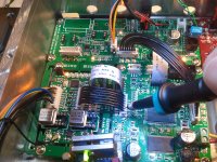
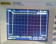
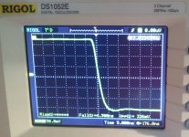
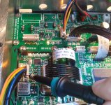
Last night I was pooking around FiFo board with my scope and found something for small R&D question.
Seems that rise and fall times for BitClock at FiFo output is about 5ns and after reclocking by ultra fast FlipFlop's rise and fall times at ClockBoard output goes UP to about 10ns...!?
I could expect rather opposite ..
Not that it can influence SQ in any way but just find it bit puzzling.
Rosendorfer
Attachments
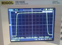
Hi Ian
Last night I was pooking around FiFo board with my scope and found something for small R&D question.
Seems that rise and fall times for BitClock at FiFo output is about 5ns and after reclocking by ultra fast FlipFlop's rise and fall times at ClockBoard output goes UP to about 10ns...!?
I could expect rather opposite ..
Not that it can influence SQ in any way but just find it bit puzzling.
Rosendorfer
Hi Rosendorfer,
You did very interesting test.
Actually, without the serial resistor, the tr and tf are mainly decided by the output dynamic current. While, with that source impedance matching resistor, the tr and tf will be mainly decided by the capacitive of the load. tr and rf are not constant, they have big relationship with the circuit parameters.
The PicoGate FF on the clock board is rated at 550 MHz with testing condition at 3.3V Vcc and 5pf CL and without Rs. So the worst case tr and tf should be better than 2.2ns. However, if you increased CL to 30Pf, the worst case tr and tf will become 5ns. But to measure tr and tf accurately at ns level, oscilloscope with mare than 1GHz bandwidth is required.
Different from the PicoGate FF, each output port of the FPGA has an internal driver, so the output current will be higher than a flip-flop. However, the high dynamic current will result in high EMI noise on the ground floor, that’s why I have to include a secondary re-clock flip-flop with independent low noise PSU on the clock board. The rated peak-peak jitter of an output of FPGA could go up to 300ps, but the output phase noise of a flip-flop will be roughly only 6dB worth than the MCLK. You might be already noticed the difference on the waveform noise from your testing result even the 50MHz bandwidth still not big enough.
You can try to output I2S signals directly from FIFO board to see if there is any sonic difference. A DS DAC usually does not sensitive to the I2S jitter (will sensitive to MCLK jitter), but a NOS DAC does.
Thank you for sharing you experience.
Have a nice weekend.
Ian
Last edited:
- Home
- Source & Line
- Digital Line Level
- Asynchronous I2S FIFO project, an ultimate weapon to fight the jitter