I think you could simply replace 74HC125 with 74ABT125[..] My first idea was to use an octal buffer like 74ac541 or 74F244 after the fifo - because the tda are in 8 pairs, each pair would get a driver. But I figured this would also negate some of the benefits of the fifo ?
Then ppl mentioned the logic level problem and I realised there were going to be too many reasons why it wasn't going to work well and I don't have the skills, knowledge or equipment to find and fix the problems[...]
These ABT logic families are quite good:
- 5V supply, with LVTTL compatible (VIH 2V) inputs
- High output capability: HIGH 32 mA; LOW +64 mA - seems more then enough to drive 16 x TDA1541 as it's specs says that digital input current for low (0.8V) -0.4mA to high (2.0V) 20uA so 16 x 0.4 = 6.4mA source capability.
- low propagation delays: ~3ns
You could give this a try.
In honor of J.S. Bach
.. thread starts at http://www.diyaudio.com/forums/power-supplies/212476-well-regulated-power-supply.html#post3019750
Andrea
would be very useful to have a thrad for this topic, the powersupplies are the real hassel building a DAC.
.. thread starts at http://www.diyaudio.com/forums/power-supplies/212476-well-regulated-power-supply.html#post3019750
Andrea
I think you could simply replace 74HC125 with 74ABT125
These ABT logic families are quite good:
- 5V supply, with LVTTL compatible (VIH 2V) inputs
- High output capability: HIGH 32 mA; LOW +64 mA - seems more then enough to drive 16 x TDA1541 as it's specs says that digital input current for low (0.8V) -0.4mA to high (2.0V) 20uA so 16 x 0.4 = 6.4mA source capability.
- low propagation delays: ~3ns
You could give this a try.
Thanks for the advice !
qusp,
Believe me if Ian makes a board that plugs into a stereo pair of PCM1704 allows NOS and 352.8 with fifo crystal level jitter he will have a gold mine, there is little money in integrating these budget S-D chips because there are several other options out there (not quite as good as Ian's but damn close.) No one is calling you selfish you are a valuable member here, but look at the big picture. Do you see people spending 5 figures + on commercial Sabre's? Since the PCM1704 has become short supply with high end DAC makers dropping them, the prices of used totl commercial 1704 dac's have skyrocketed. Have you ever listened to a properly built PCM1704 (I mean no DF1704, top notch power supplies, top notch analog stage)?
The reason we are bringing up the 5V TLL is this second version is supposed to plug into the most popular digital filter ever (PMD100), if the level is an issue better to know now than before customers find out.
I also support increasing the price of the gb boards if needed, this from the start has potential to change the way we think about DIY DAC's.
Priority is simple and not as complex as you think:
1. stereo PCM1704 up to 8xfs
2. TDA1541 RBCD (check done complete)
3. ESS9018 (check done complete)
4. PMD100/SM5842 RBCD (close needs tested)
5. PCM56/AD1865/AD1862 RBCD
That pretty much covers all the high end DAC's made (I put the ESS on there for your impaired hearingLeft off the TDA1543 as this from development was a budget chip, people have done creative things to overcome this but probably will always have to do so. This doesn't have to be a ******* match of my DAC vs yours, just 5 simple priorities that will change the way we DIYers build D/AC's forever.
Good ideas!
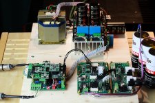
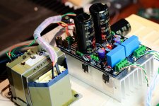
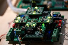
FIFO and ESS9018(Buffalo III) hookup
I just got time this weekend playing with my ESS9018 DAC.
My system:
B&W 804, Pass A5, Pass 1.7, Buffalo III, LegatoIV,SalasShuntReg...
At beginning, I fed opt S/PDIF directly into BIII. It sounds pretty good, better than many other DACs at the same condition (without FIFO and good clock). That means the internal DPLL and jitter reduction is working. However, there are some click noises occasionally when Fs goes up to 192Khz.
Then I connected the FIFO I2S output into BIII via U.FL coaxial cables. Same opt S/PDIF into S/PDIF Interface Board. FIFO was powered by a battery pack with 22.5792 and 24.5760 CCHD957 attached on the Dual XO Clock board. The result was quite impressed. I don’t want to say it’s perfect, but I have to say it’s very close to. I tried a couple of different kind of XO and found that the sound of ESS9018 still quite sensitive to the jitter from the input digital audio stream. I suspect the internal DPLL still has to trace the input clock to get lock with it. So, the clock jitter, outside the DPLL bandwidth, will still be introduced into DAC, which usually, the close in phase noise. While the final phase noise within the DPLL bandwidth will be decided by the performance of the internal DPLL(phase noise floor).
No click noise at all with same 192Khz input.
Next step, I’ll try the synchronized mode. But I have to remove the on-board CCHD950 100Mhz oscillator.
Have a nice week.
Attachments
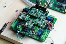
Ian,
Nice photos! Had me confused for a second there looking at your power supplies, I didn't spy the 3rd salas reg that is hanging off the side of the heat sink.
Looks to me like you need a D1 to complete the set so you don't need to worry about any of those other DAC chips
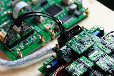
Could you give any details on how you're terminating that i2s from u.fl into the pin female pin header? Have you had any thoughts on how to improve the situation at the DAC end of that interface? I've had thoughts about making a small pcb to convert pin headers to u.fl sockets and would appreciate your thoughts/experiences. I guess there is probably a bunch of other people in this thread looking to interface this board to DACs that don't always have ideal methods for connecting the i2s signal.
Nice photos! Had me confused for a second there looking at your power supplies, I didn't spy the 3rd salas reg that is hanging off the side of the heat sink.
Looks to me like you need a D1 to complete the set so you don't need to worry about any of those other DAC chips
Could you give any details on how you're terminating that i2s from u.fl into the pin female pin header? Have you had any thoughts on how to improve the situation at the DAC end of that interface? I've had thoughts about making a small pcb to convert pin headers to u.fl sockets and would appreciate your thoughts/experiences. I guess there is probably a bunch of other people in this thread looking to interface this board to DACs that don't always have ideal methods for connecting the i2s signal.
Last edited:
nice work Ian, you dont have to remove the clock for sync mode, you can just remove the ferrite that disables the regulator for it and then easy to solder a u.fl in front of the clock, between the XO and the 9018 there is pads or at least there was on bII for a resistor R17. pretty sure even on b3 there is a position to do this, check out Leon's upgrade manual. yes the clock will still be there and will be in HiZ mode, but it still works. however since you'll be using it with external clock all the time and have the tools to remove it go ahead. maybe heatsink the chip though while you are doing it.
yes Ian, you need to play with some other IV stages to take it the next level, the D1 is highly recommended =)
yes Ian, you need to play with some other IV stages to take it the next level, the D1 is highly recommended =)
Hi Ian,I just got time this weekend playing with my ESS9018 DAC.
My system:
B&W 804, Pass A5, Pass 1.7, Buffalo III, LegatoIV,SalasShuntReg...
At beginning, I fed opt S/PDIF directly into BIII. It sounds pretty good, better than many other DACs at the same condition (without FIFO and good clock). That means the internal DPLL and jitter reduction is working. However, there are some click noises occasionally when Fs goes up to 192Khz.
Then I connected the FIFO I2S output into BIII via U.FL coaxial cables. Same opt S/PDIF into S/PDIF Interface Board. FIFO was powered by a battery pack with 22.5792 and 24.5760 CCHD957 attached on the Dual XO Clock board. The result was quite impressed. I don’t want to say it’s perfect, but I have to say it’s very close to. I tried a couple of different kind of XO and found that the sound of ESS9018 still quite sensitive to the jitter from the input digital audio stream. I suspect the internal DPLL still has to trace the input clock to get lock with it. So, the clock jitter, outside the DPLL bandwidth, will still be introduced into DAC, which usually, the close in phase noise. While the final phase noise within the DPLL bandwidth will be decided by the performance of the internal DPLL(phase noise floor).
No click noise at all with same 192Khz input.
Next step, I’ll try the synchronized mode. But I have to remove the on-board CCHD950 100Mhz oscillator.
Have a nice week.
Nice finding. Thanks for sharing. I have a BII and am using the same connection (SPDIF -> FIFO -> SPDIF -> BII). Nothing much to worry about as it is just simple 1 line connection.
I'm thinking of using I2S input and sync mode for next upgrade. But the I2S connection going to be long as DAC + FIFO is in 1 casing, HiFace is in another casing. I am thinking of using Twisted Pear - Teleporter. This will be my next project before D1.
-coolhead
have they made it so you cant use an external clock without removing it with the B3? with B2 you could just leave it unpowered by removing the ferrite that connects to the clock reg and connect the clock to the vacant pad at R17 (actually perfect for soldering a u.fl socket to as I did) the datasheet for the crystek would have you thinking this wouldnt work as the clock is in HiZ mode in shutdown, but this isnt the case it works fine.
since you'll be using the b3 with an external clock exclusively and have the tools to remove the XO fairly easily, its not a big deal I guess, but for the average user thats a bit annoying they've removed that ability to easily use an external clock with the update.
coolhead: so you already have the hiface? your proposed solution sure doesnt sound ideal, teleporter will not be jitter free either. IMO you would be better off getting lorien's Xmos USB->i2S board and connecting it directly to the fifo. it can be powered by USB or batteries, so shouldnt take up much space. even though the fifo definitely helps a great deal with solving jitter on MCLK, I think its better for it not to be there to begin with.
Last edited:
At beginning, I fed opt S/PDIF directly into BIII.
Can you repeat this experiment feeding it i2s?
Can you repeat this experiment feeding it i2s?
read his post, he already has
or do you mean an intermediate step feeding direct i2s without fifo?
coolhead: so you already have the hiface? your proposed solution sure doesnt sound ideal, teleporter will not be jitter free either. IMO you would be better off getting lorien's Xmos USB->i2S board and connecting it directly to the fifo. it can be powered by USB or batteries, so shouldnt take up much space. even though the fifo definitely helps a great deal with solving jitter on MCLK, I think its better for it not to be there to begin with.
Hi qusp,
Yup, i am using the HiFace as transport for sometime already. I haven't order the Teleporter yet, being thinking about it for some time. I am still open to idea.
This is my plan: To fit all 4 modules (hiface, FIFO, BII, D1) into 1 casing would be ideal, but space is really a concern, I also have salas shunt regulators for them. Another option would be remove all power supply to another casing, as it has remote sensing, distance wouldn't be a problem.
I think for future flexibility also, it make sense to combine only 3 modules (FIFO, BII, D1) into 1 casing as I have the flexibility to try other transport in future.
PS: to make thing more complicate, I have a spare BII board, I can do duo mono also.
Thanks.
-coolhead
It is obvious that a PLL recovered clock will greatly benefit from the FIFO. I was just wondering how much an I2S stream will be improved by the FIFO as compared to directly feeding it to the Sabre.
fair question, suppose it depends on the quality of the i2s source
...
Next step, I’ll try the synchronized mode. But I have to remove the on-board CCHD950 100Mhz oscillator.
Have a nice week.
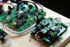
Very nice photos.
What setting for the DPLL did you use? for the different sample rates?
Very nice photos.
What setting for the DPLL did you use? for the different sample rates?
Thanks glt,
I use BIII default setting so far with all the switch jumpers at off position. I don't think this optimized for all the sample rates. What suggestion do you have?
I suspect, internally, ESS9018 has the similiar ASRC architecture with AD1896. But to run the 1896 at master-mode, you not only have to feed the I2S synced with the MCLK but also you have to set the corresponding jumper as well. For ESS9018, does it switch to sync mode(or master mode) automatically if the input I2S already sync with the MCLK(256,512 or 1024*fs)?
...
I use BIII default setting so far with all the switch jumpers at off position. I don't think this optimized for all the sample rates. What suggestion do you have?
use "lowest" Block 1 switches 5, 6, 7: On, OFF, OFF
When I use "lowest" and the source is a FPGA based I2S, I have to wait about one hour for the DAC to warm up; otherwise I get drop-offs (the DPLL looses synch)
...
I suspect, internally, ESS9018 has the similiar ASRC architecture with AD1896. But to run the 1896 at master-mode, you not only have to feed the I2S synced with the MCLK but also you have to set the corresponding jumper as well. For ESS9018, does it switch to sync mode(or master mode) automatically if the input I2S already sync with the MCLK(256,512 or 1024*fs)?
Automatically.
"Dustin: Again true but not the whole story. You can use the ASRC if you like - or not by simply clocking the XIN pin synchronously (at an integer multiple) to the BCLK. Then the ASRC drops itself out, reverting in this case to a more conventional method as the other DACs I'm aware of do."
6moons audio reviews: Wyred4Sound DAC2
use "lowest" Block 1 switches 5, 6, 7: On, OFF, OFF
When I use "lowest" and the source is a FPGA based I2S, I have to wait about one hour for the DAC to warm up; otherwise I get drop-offs (the DPLL looses synch)
Automatically.
"Dustin: Again true but not the whole story. You can use the ASRC if you like - or not by simply clocking the XIN pin synchronously (at an integer multiple) to the BCLK. Then the ASRC drops itself out, reverting in this case to a more conventional method as the other DACs I'm aware of do."
6moons audio reviews: Wyred4Sound DAC2
Thanks, I'll give a try.
Ian,
Nice photos! Had me confused for a second there looking at your power supplies, I didn't spy the 3rd salas reg that is hanging off the side of the heat sink.
Looks to me like you need a D1 to complete the set so you don't need to worry about any of those other DAC chips
Could you give any details on how you're terminating that i2s from u.fl into the pin female pin header? Have you had any thoughts on how to improve the situation at the DAC end of that interface? I've had thoughts about making a small pcb to convert pin headers to u.fl sockets and would appreciate your thoughts/experiences. I guess there is probably a bunch of other people in this thread looking to interface this board to DACs that don't always have ideal methods for connecting the i2s signal.
Thanks hochopeper,
Like my Salas shunts
? The temperature goes up to 60 degree C after 2 hours running, is that safe enough?I just cut the 12" u.fl cables right in the middle, peeling off it at the end, separating the shield into a GND wire in a heat-shrink, then solder them into a pair of female pins and plug them into a 2 pos house. Making a adapter board with u.fl socket will be better for hookup, but I didn't see big difference on performance. The best way is solder the u.fl direct to the board as qusp did, but how about those already has the connecter soldered on board
?Can you repeat this experiment feeding it i2s?
It is obvious that a PLL recovered clock will greatly benefit from the FIFO. I was just wondering how much an I2S stream will be improved by the FIFO as compared to directly feeding it to the Sabre.
Hi analog_sa,
I did the test, the reslut was quite interesting.
When I switched the I2S source from FIFO output to S/PDIF board output(bypass FIFO), BIII still sounds wonderful, not as worse as I thought. However, when I switched the I2S back to the FIFO output, I heard the difference, very obviously, especially at high and middle-high range.
But it's just my personal feelings, so if it's possible, try it by yourself
. The FIFO XO was 22.5792Mhz CCHD957 for the test. ESS9018 was at ASRC mode(with 100MHZ CCHD950 for local MCLK).
Have a good night.
- Home
- Source & Line
- Digital Line Level
- Asynchronous I2S FIFO project, an ultimate weapon to fight the jitter