While I wait for reviews on the FPGA module that will be included in my next DAC, I am thinking about the next step in the project.
The idea is to get a DAC development platform, which which will allow anyone willing to participate, to build modules, exchange them (by mail) via other participants, and share listening results. The purpose of this project is to make some sort of standard pinout for little DAC or I/V daughterboards, so that all of you people can exchange little modules.
This will allow comparison of various DAC chips or I/V schemes, all other things being equal. It should be interesting...
This "platform" will be a board, with several connectors on it, to plug modules. It will have an on-board Tent clock, supply decoupling, audio outputs, and some power supply regulators. It should not have too much stuff, because ideally everything should be a plugin, to allow for more experimentation.
It will have its own clock to eliminate jitter issues and the issue of everyone having a different digital source. Therefore, it will have a clock output and an I2S input for slaving the source. I am doing this for my Ethernet audio project, so the board will connect to the Ethernet FPGA module. It will also have a slot for an ASRC and a SPDIF input, so anyone will be able to experiment with it provided they have a SPDIF source at hand.
The modules I am thinking about are :
- SPDIF Input and ASRC
- Digital Filter
- DAC
- I/V
- Balanced to Unbalanced (for balanced-out DACs)
- Lowpass filter (if needed)
- Volume control
- Output buffer
So basically this is just a board with 8 connectors, a power supply input, a clock, decoupling, and some RCAs for audio output. Modules will be daughterboards plugged in at a 90° angle. The board itself is really nothing special, the important thing is that everyone works with coherent pinouts to be able to share modules.
So :
- Who is in ?
- Who has other ideas for other modules ?
- Who can suggest a cheap, and practical connector solution ?
I was looking at board-edge connectors. This would make module boards very simple, having simply an their edge pushed in a female connector on the main board. Leveraging the economies of scale of the PC platform is a good idea : PCI and PCI-Express connectors are quite cheap. The drawbacks of this approach is that the width of a module board is fixed, some connectors need a lot of holes in the PCB (PCI has too many pins) and PCI-Express needs the module boards to be milled to shape.
I an thinking about using 90° Sub-D connectors. These are dirt-cheap and work well. The main board would have straight female connectors and the modules would have 90° male connectors. There is no restriction on module board size.
WHat do you think ?
Great concept. And at the right time - i've just been scratching my head over where to test an AD1955. Such a unified test bed will greatly help in comparisons and development.
An unwanted ASRC module, per example, can just get replaced with a shorting plug.
DB9 connectors are probably all that is required. They are low-tech but cheap, easily available and most importantly allow for improvised prototyping plug-in modules.
I would like to see the option for multiple independent power supplies, rather than a shared raw dc. At least one single PS per module with local regulation on the daughter boards. Higher performance regulation (Jung) may also be available on plug-in modules for the analogue stages. Not sure if this is practical.
As many won't have use for spdif inputs a USB input module should be easy to fit in place of spdif. This means the USB/SPDIF slot needs to be positioned appropriately regarding access to the port.
I have just built a Audio Note Dac1 kit and plan to a few experiments
a) using I2S rather than Spdif. (See my I2S thread)
I have located the I2S signals in an Arcam Cd72's Sony drive mechanism and will use an Atmel At Tiny44 instead of glue logic to
'convert' the 24bit drive output to 18bits for the dac.
b) I also plan to parallel 4 AD1865s* to increase the output current by piggy backing them. Though it will require mods to the onboard 5v regulators.
*These are still available from Digikey for about £10
I feel the Dac1.1 kit is a good basis for experiementing - penty of room in the enclosure, valve output stage with scope for upgrading, dac pcb with socketed CD8416 and AD1865, Audio Note interstage transformers are available for £70 for a further upgrade (couple the dac out to valve input)
This is my first foray into digital audio but from the detail and clarity improvement already provided by the Dac1, I'm 'hooked'!!
P
Nice idea, I wanted to do this years ago (connectors are still in the drawer  )
)
I would vote for:
removing the volume control and output buffer. This has little to do with the idea itself
adding USB input module
adding power supply module
You should "design" first a BUS "Standard" where all possible signals and power supplies are present, so every one can design any module according to this standard.....
If everyone would except this standard, every one can build a masterboard and modules ....
AND, you need to set up a seperate WEB Site for this, otherwise it will run dead for sure...
)I would vote for:
removing the volume control and output buffer. This has little to do with the idea itself
adding USB input module
adding power supply module
You should "design" first a BUS "Standard" where all possible signals and power supplies are present, so every one can design any module according to this standard.....
If everyone would except this standard, every one can build a masterboard and modules ....
AND, you need to set up a seperate WEB Site for this, otherwise it will run dead for sure...
I'm totally into this one, I've been thinking about doing something like this for the past couple months... Here are a couple ideas I have for something like this...
I think there should be at least 2 board-board connectors; 1 for power, 1 for signal.
I think each board should have a (3?)-bit ID which could be set via DIP switches or read serially via an on board eeprom. Any board could send or receive I2S audio from the base board for distribution to other boards... For my personal application, i'd like to have enough room to carry around 3 sets of I2S so that 5.1 could be achieved... daughter boards that use the I2S as input should have DIP swtiches to select which channels to use for whatever output method is going on (IE: headphone amplifier.)
I don't think the PSU should be a module, but part of the base main board... or have alternative inputs for PSU... so that the base is more of a platform [which includes the PSU]
I thought of making this a vertically stackable system -- each board has a top and bottom connector for expansion. The bottom board would be PSU (PSU caps would be on the bottom of the first board, with standoffs to a case.) The second board would be the FPGA/logic-level stuff that includes an LCD display, rotary encoder and a couple buttons. The third board and beyond would be configurable to taste. I like the vertical method; however, the disadvantage lies in the fact that each board would be required to be within the size of the base.
If more than one board were an input IE: a board that could do USB in, Optical in, and SPDIF in, the board would have 3 ID assignments and would enable or disable tristate buffers to be in high impedance mode to allow one set of inputs flow to the other devices.
The PSU would push around standard levels; 12, 5, 3.3, 1.2-1.8 (for FPGAs) and ground. If a module needed a significant amount of current, or a specific voltage, either cables could provide it via external connector input or through extra pins left on the PSU board-board connectors and specialized powersupply below the logic/low-current powersupply.
These are all just ideas, kicking them around... I might throw together some sketches
I'm interested, count me in.
How about a high quality clock source on the board as well? Just change a crystal and a couple of caps as needed for the specific clock frequency required.
Several power buses - all modules probably should have local regulation as well.
DB9 characteristic impedance might not be the optimum choice for digital bus - any thoughts on this?
Provision for ISO150 for breaking loops. (dac end of board)
First things first, this kit will not support multichannel for active crossover. The purpose is to compare DACs after all... and with multichannel the connector issues become a huge headache.
The more I think about this setup, the more I start to prefer a layout where boards all lay flat on the table, connected through edge connectors, like this :
For edge connectors I could simply use the good old DB25. And making the power supply connections where shown on the diagram should be OK.
* Board 1 : Digital Audio IO
This will be a double-sided board, this means board space is cheap, so I will include as much crap as possible on this one, I'll make a complete board, then whoever wants one just solders what he needs. Contents :
- Supply regulator, since everything here runs at +3.3V, a simple LM317 should do the trick.
- CS8416 (SPDIF In, transformer isolated, switchable SPDIF inputs)
- PCM2704 to have an USB source, it will output SPDIF that will be redirected to CS8416 via a transformer.
- CS8406 (SPDIF Out, transformer isolated), yes this is for slaving a soundcard to the DAC master clock.
It will output digital silence unless someone bothers to make an ADC module... now where would I put that ?
SPDIF out will be the usual RCA.
- Master clock output (transformer isolated).
This is for slaving a CD player. I will probably put a RJ45 or SATA connector, to have two twisted pairs : one to send the clock to the player, one to get the SPDIF back. SATA is nicer I think.
- AD1896 ASRC
This will only be needed if the source is not synchronized with the DAC clock : raw SPDIF, and USB. I have a "free sample" somewhere so I may as well include it.
- Connector
This will connect to the next module.
It will carry :
- Power, Ground
- Digital Audio signals obviously : I2S in, I2S out, ASRC out, master clock
- I²C to talk to the chips
The chips will be in software mode, after all there is a CPU on the next module.
By the way the SPDIF transformers will be LAN magnetics (HX1198).
Questions :
=> Do I need to add space for an optical SPDIF I/O ?
=> how many SPDIF inputs do you vote for ? I'd say 1 directly wired to the USB chip, 1 on the SATA connector, and 2 extra on RCAs.
* Next module : the CPU
This should handle audio samples FIFO, oversampling with your choice of impulse responses, and I2C configuration of the rest of the chips, including the DACs (since if you oversample outside the DAC you have got to tell it to adjust its settings), etc.
At first I wanted to make a simple FPGA design that doesn't need a super-expensive PCB prototype like my ethernet module does, so I thought about putting a Spartan-3E 100 for oversampling and an Atmega64 for the rest. However this would mean two software forks... So, instead, since I ordered the parts too early for the ethernet module I have 2 extra XC3S500E in PQ208 package, so I might as well use that, since those are manageable on a 4-layer board which is a lot cheaper. So, I can hit two birds with 1 stone, that is make a module that will be useful, put to use parts that would otherwise go in the junk bin, and practice the FPGA skillz.
So the CPU module could be :
- Spartan-3E 500 on 4-layer board, CPU is Microblaze
- Flash for configuration and firmware
- RS232 port
- Extra IO connector for LCD and buttons
This way I can reuse all software and make target practice on the hardware at the same time. Since I wanted to put a LCD on my DAC and a few buttons for user interface, I'll implement it now instead of later, so there is no loss of effort.
* Clock module
This just contains a Tent clock, a few latches for reclocking, and a regulator. The master clock is sent to the CPU module.
To test several regulators for the clock PSU, just build several modules. I will probably socket the Tent clock since it's expensive.
This leaves the door open for replacing the clock with a VCXO and using a software PLL run by the Microblaze, which would obsolete the ASRC.
* DAC module
Just a DAC and regulators... since all DACs use different supply voltages it makes sense to put the regulators there too.
There will also be a small I²C EEPROM so the CPU module knows what's plugged in and how to talk to it.
* Analog modules (to the right)
I will try to use a connector pinout that supports daisy-chaining. That means, if you use a DAC with voltage output, you don't plug anything afterwards, just an output connector. If you use an AD1955 you'll need an I/V, lowpass, and balanced -> unbalanced conversion.
The power supply paths (see block diagram above) should be OK I think.
So, what do you think ?
The more I think about this setup, the more I start to prefer a layout where boards all lay flat on the table, connected through edge connectors, like this :
An externally hosted image should be here but it was not working when we last tested it.
For edge connectors I could simply use the good old DB25. And making the power supply connections where shown on the diagram should be OK.
* Board 1 : Digital Audio IO
This will be a double-sided board, this means board space is cheap, so I will include as much crap as possible on this one, I'll make a complete board, then whoever wants one just solders what he needs. Contents :
- Supply regulator, since everything here runs at +3.3V, a simple LM317 should do the trick.
- CS8416 (SPDIF In, transformer isolated, switchable SPDIF inputs)
- PCM2704 to have an USB source, it will output SPDIF that will be redirected to CS8416 via a transformer.
- CS8406 (SPDIF Out, transformer isolated), yes this is for slaving a soundcard to the DAC master clock.
It will output digital silence unless someone bothers to make an ADC module... now where would I put that ?
SPDIF out will be the usual RCA.
- Master clock output (transformer isolated).
This is for slaving a CD player. I will probably put a RJ45 or SATA connector, to have two twisted pairs : one to send the clock to the player, one to get the SPDIF back. SATA is nicer I think.
- AD1896 ASRC
This will only be needed if the source is not synchronized with the DAC clock : raw SPDIF, and USB. I have a "free sample" somewhere so I may as well include it.
- Connector
This will connect to the next module.
It will carry :
- Power, Ground
- Digital Audio signals obviously : I2S in, I2S out, ASRC out, master clock
- I²C to talk to the chips
The chips will be in software mode, after all there is a CPU on the next module.
By the way the SPDIF transformers will be LAN magnetics (HX1198).
Questions :
=> Do I need to add space for an optical SPDIF I/O ?
=> how many SPDIF inputs do you vote for ? I'd say 1 directly wired to the USB chip, 1 on the SATA connector, and 2 extra on RCAs.
* Next module : the CPU
This should handle audio samples FIFO, oversampling with your choice of impulse responses, and I2C configuration of the rest of the chips, including the DACs (since if you oversample outside the DAC you have got to tell it to adjust its settings), etc.
At first I wanted to make a simple FPGA design that doesn't need a super-expensive PCB prototype like my ethernet module does, so I thought about putting a Spartan-3E 100 for oversampling and an Atmega64 for the rest. However this would mean two software forks... So, instead, since I ordered the parts too early for the ethernet module I have 2 extra XC3S500E in PQ208 package, so I might as well use that, since those are manageable on a 4-layer board which is a lot cheaper. So, I can hit two birds with 1 stone, that is make a module that will be useful, put to use parts that would otherwise go in the junk bin, and practice the FPGA skillz.
So the CPU module could be :
- Spartan-3E 500 on 4-layer board, CPU is Microblaze
- Flash for configuration and firmware
- RS232 port
- Extra IO connector for LCD and buttons
This way I can reuse all software and make target practice on the hardware at the same time. Since I wanted to put a LCD on my DAC and a few buttons for user interface, I'll implement it now instead of later, so there is no loss of effort.
* Clock module
This just contains a Tent clock, a few latches for reclocking, and a regulator. The master clock is sent to the CPU module.
To test several regulators for the clock PSU, just build several modules. I will probably socket the Tent clock since it's expensive.
This leaves the door open for replacing the clock with a VCXO and using a software PLL run by the Microblaze, which would obsolete the ASRC.
* DAC module
Just a DAC and regulators... since all DACs use different supply voltages it makes sense to put the regulators there too.
There will also be a small I²C EEPROM so the CPU module knows what's plugged in and how to talk to it.
* Analog modules (to the right)
I will try to use a connector pinout that supports daisy-chaining. That means, if you use a DAC with voltage output, you don't plug anything afterwards, just an output connector. If you use an AD1955 you'll need an I/V, lowpass, and balanced -> unbalanced conversion.
The power supply paths (see block diagram above) should be OK I think.
So, what do you think ?
These are deep waters for me to really express an opinion but what the hell ")
What fights jitter in this design? An ASRC, a potential VCXO secondary PLL or a software PLL. No idea how all of these compare but i feel none will actually give us a carte blanche to ignore input jitter. I know this is certainly true for the ASRC.
I have no particular interest in spdif but using a Crystal receiver (Schmitt triggers) mandates an input buffer of sorts, even if it only a 74hcu04. IME it is more important for good sound than the spdif transformer. Two regulators are also essential.
My main source is currently a PC using a USB port. Having compared a USB/spdif conversion to direct I2S connection i would say there is no contest. Jim Hagerman is obviously of a different opinion as he has lots of faith in his secondary PLL but i suspect convenience and simplicity are the main factors behind his solution. Please, lets use at least a 2707 with i2s outputs, even if it means complicating the switching arrangements.
Mega64 code i can probably maintain and modify; the Spartan sounds like a serious learning curve which may be fun. Or not.
If the Spartan chip is responsible for IIC and other housekeeping tasks this might be awkward for many diyers.
Actually what fights jitter in this design is that the source (in my case PC via ethernet) is synchonized with the DAC and not the other way. I don't use a PLL or anything, it's just synchronous.
The other preferred solutions are : slaving the computer soundcard (easy to do with SPDIF, I did it, it works), and slaving a CD player (I also tried it).
In all above cases, there is a "core", ie. main clock, reclocking latch, and DAC, and the rest (ie the source) works in sync, so there is no clock recovery problem because there is no clock recovery at all...
But since this is a project that should involve people trying various DACs and building modules themselves, I'd like to leave all doors open. Hence the option for other sources, the ASRC, and the USB DAC. But those are not optimal, I know. Perhaps I should remove the USB thingie. But I'd like to include it as a challenge...
As for the ease of use of the Spartan chip, I'll do the HDL, but the C code is pretty easy to do. I especially like live debugging over JTAG.
Can you source a 2707 ?
Originally posted by peufeu
The other preferred solutions are...
I'd like to add a request for a simple BNC clock output (for when using a "proper" soundcard with a clock input), if that's possible. Shouldn't need much in the way of extra hardware, I don't suppose.
Originally posted by peufeu
As for the ease of use of the Spartan chip, I'll do the HDL, but the C code is pretty easy to do.
You can program FPGAs in C? I didn't know that... that would make it much easier to break into the FPGA world (which I'm really itching to do), since I don't know VHDL or Verilog and they look quite weird to me...
If your soundcard has a clock input, it's most likely a wordclock input... can you give me the specs (voltage mostly), the frequency will be 44.1k right ?
As for the FPGA, you use Verilog or VHDL to program them (it's quite interesting) but using the Xilinx tools you can instantiate a processor (microblaze) which is then built using the FPGA fabric ; then you can write peripherals for it in verilog or VHDL and write C code for the processor. For instance in my ethernet DAC prototype, the stuff like I2S encoders and DMA is written in verilog, but the UDP packet parsing is written in C...
As a CPU the microblaze isn't that powerful but what's nice is the integration and how you can mix it with custom hardware.
peufeu said:
=> Do I need to add space for an optical SPDIF I/O ?
- I'd like at least one optical input.
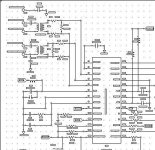
Complete schematics and routed PCBs of the digital IO module with the features listed above :
http://home.peufeu.com/nik/dac/DigitalIOBoardv01.pdf
Feel free to have a look
http://home.peufeu.com/nik/dac/DigitalIOBoardv01.pdf
Feel free to have a look
Just a couple of quick thoughts, might be a good idea to return the transformer secondaries directly to RXN on the CS8416 - I don't think you want to share the local noisy ground plane with your incoming low level spdif signals.
I haven't had time to review in detail, but the design looks very interesting and well thought out in general.
Some series terminating resistors for reflections on the output of the CS8416 and anything else sending to the edge card connector would be something I would add. Possibly buffer these?
More later..
Attachments
- Status
- This old topic is closed. If you want to reopen this topic, contact a moderator using the "Report Post" button.
- Home
- Source & Line
- Digital Line Level
- The DAC development platform