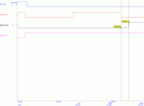
Attached is a simulation ran on your circuit.quantran said:In both schematic, data is delayed by 1/2 BCLK cycle plus the propagation delay caused by the logic chip. Propagation delay time is given in datasheet as max limit only. In fact propagation delay time is normally shorter than max limit and also depends on brand of logic IC so we do not know exactly whether the propogation delay time is long enough for the receiving IC to work.
As you can see, SDATA is being delayed 1BCLK + 29n which should work just fine.
I also ran a sim on my idea, and of course you are right, it was delayed only 1/2 BCLK + some delay, which of course is not what I actually need.
Attachments
The safest way to do this cleanly is clock twice, falling edge with the first flop, then rising edge with the second, to delay the data by 1/2 cycle and then another 1/2 cycle. This has the least sensitivity to timing skew as the data setup and hold times are maximal at 1/2 a BCLK cycle.
To be absolutely paranoid you'd delay LRCLK by 1 cycle and DATA by 2 cycles, each using the above technique - this re-establishes precise timing relationship between BCLK, DATA and LRCLK, although it doesn't buffer BCLK (or improve its jitter)
To be absolutely paranoid you'd delay LRCLK by 1 cycle and DATA by 2 cycles, each using the above technique - this re-establishes precise timing relationship between BCLK, DATA and LRCLK, although it doesn't buffer BCLK (or improve its jitter)
Dear Mark, thx for quick answer. If so i would try it if its possible with best result (paranoid)
Can you tell me a shematic how to do this. I am an experienced solderer.
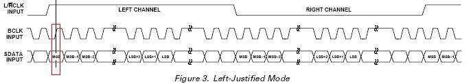
I want to connect a SkySong XU208 USB to I2S Board that outputs me standard i2S to my Mytek DSD 192 DAC. Note: I removed TAS1020 USB 1.1 chip and attached BitClock WordCLK and Data. It works all fine also sampling frequence changes, but sound is disturbed. The designer of the DAC told me that they use left justified I2S.
Can you tell me a shematic how to do this. I am an experienced solderer.
I want to connect a SkySong XU208 USB to I2S Board that outputs me standard i2S to my Mytek DSD 192 DAC. Note: I removed TAS1020 USB 1.1 chip and attached BitClock WordCLK and Data. It works all fine also sampling frequence changes, but sound is disturbed. The designer of the DAC told me that they use left justified I2S.
It means what I want it to mean when I want it to mean it.
If you take a look at page 2-21 of the TAS1020 datasheet, under the heading Inter-IC Sound (I2S) Modes of Operation, it is clear that the output of the TAS1020 is I2S as per the I2S specification as opposed to some mythical chimera.
You'll find the same in the TAS1020A and TAS1020B datasheets.
If you take a look at page 2-21 of the TAS1020 datasheet, under the heading Inter-IC Sound (I2S) Modes of Operation, it is clear that the output of the TAS1020 is I2S as per the I2S specification as opposed to some mythical chimera.
You'll find the same in the TAS1020A and TAS1020B datasheets.
Last edited:
Thanks a lot rfbrw for your help.
My aim is to replace the TAS1020 "input" lane with my SkySong XU208 (Xmos) USB - I2S adapter. As reported it works but distorted.
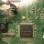
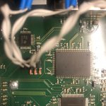
I detected pins 35,37,38 at TAS1020 as CSYNC, CSCLK and CDATO. I connected these to my SkySong XU208 XMOS adapter to FSCLK, SCLK and DATA pins.
(Note: My SkySong XU208 XMOS adapter supplies the following aoutput headers:
3,3V,GND,DSDOE,MCLK,FSCLK,SCLK,DATA,SPDIF,MUTE,D64 and F0-F3 for LED to show sampling rate and mode of operation)
The info from the designer of my Mytek DSD 192 is that they use justified left.
It would be wonderful if somebody could help me to let the SkySong XU208 XMOS adapter work with my Mytek.
Note: I desoldered Pin 35,37,38 of the TAS1020 on the Mytek PCB (I lifted the pins upwards. After that i attached thin wires to the soldering pads of the 3 lanes to connect them to the SkySong XU208 XMOS adapter. Pin 36 (SDIN) i did also remove as i thought i dont need it (DAC mode only) as i could easier work on pin 35. All the other pons of TAS1020 are still connected to the boards and some of the lanes are still connected to the same chip where pin 35,37,38 are going to (Altera).
Thanks and have a nice weekend
My aim is to replace the TAS1020 "input" lane with my SkySong XU208 (Xmos) USB - I2S adapter. As reported it works but distorted.
I detected pins 35,37,38 at TAS1020 as CSYNC, CSCLK and CDATO. I connected these to my SkySong XU208 XMOS adapter to FSCLK, SCLK and DATA pins.
(Note: My SkySong XU208 XMOS adapter supplies the following aoutput headers:
3,3V,GND,DSDOE,MCLK,FSCLK,SCLK,DATA,SPDIF,MUTE,D64 and F0-F3 for LED to show sampling rate and mode of operation)
The info from the designer of my Mytek DSD 192 is that they use justified left.
It would be wonderful if somebody could help me to let the SkySong XU208 XMOS adapter work with my Mytek.
Note: I desoldered Pin 35,37,38 of the TAS1020 on the Mytek PCB (I lifted the pins upwards. After that i attached thin wires to the soldering pads of the 3 lanes to connect them to the SkySong XU208 XMOS adapter. Pin 36 (SDIN) i did also remove as i thought i dont need it (DAC mode only) as i could easier work on pin 35. All the other pons of TAS1020 are still connected to the boards and some of the lanes are still connected to the same chip where pin 35,37,38 are going to (Altera).
Thanks and have a nice weekend
Hi there
does anybody know how to convert from I2S standard (Sky song xu208 USb to I2s) to left justified (Mytek DAC that uses Left justified) ?
Hi
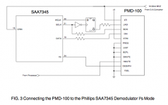
Please try simple circuit from PMD100 datasheet. (I am using this for diskrete dac with Left Justified format. Working good.) And You can use 3.3V components (match the standard for Your boards...) The circuit just hold, for one BCLK, LRlatch (WCLK marked in the schematic) line. BCLK and DATA lines are unchanged. You can use rsistors like in the schematic values are all the same, from 22ohm to 47ohms. In I2S LRlatch goes ONE BCK prior to the data set.
Attachments
Last edited:
- Status
- This old topic is closed. If you want to reopen this topic, contact a moderator using the "Report Post" button.
- Home
- Source & Line
- Digital Line Level
- Left-justified I2S to Philips I2S Converter