Hi Guys
Here it sends you right away to drilling section
This will bring you direct to assembly Section..
This will bring you to THROUGH HOLE Section
Here a small Guideline Step by Step, how someone could create his own PCB without having a lot of Technical Knowledge, (same as me).
But before we begin here, a few things which come first.
I use BUNGARD Positive Photosensitive PCB's. There are different Manufacturers, but for me, the ones with that light blue protection sheet are the one which, seems to make the least hassles..
Precautions.:
You are working with Chemicals, so protect yourself as good as you can.
Use thin rubber gloves, use if ever possible a separate room.
Do not inhale fumes from developing solution or while etching the PCB from etching solution.
Use Clean environment.
Work in good ventilated rooms or outside on the balcony or where ever you have lots of fresh air.
RTM
Read the manual of the PCB Manufacturer and also read what can go wrong and why it goes wrong, meaning bad and not usable output..
First Comes First: ARTWORK
But first you need to create your artwork, Single side or double side makes actually not a big difference, except that if you want to make double sided PCB, the fact is if you fail on either side you have to throw away the PCB as a whole..
A few word for manufacturing:
Keep in mind that Temperatures of all the components play a big role but also surrounding temp in your room.
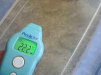
For German manufacturers like Bungard, they give a lead of 20 Degrees Celsius, but not over 22 and not UNDER 20 so be exact there.
Tools you need
A Good BEAM Temp Meter where you can be sure that it measure the temp on 0.1 Degree, never mind if this is Water or Ice, Stone, Iron, Aluminum never mind the color the surface has.. ( there are cheap Temp Measuring tools out there, depending on color these will not read the correct temp.
A few plastic containers, to develop and Etch the PCB-.
Thin rubber or silicone Hand gloves.
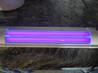
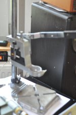
A Ultra Violet Lamp or Exposing unit. Minimum 40 Watts
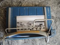
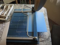
A good Paper Cutting Machine where it enables you to also cut PCB's. (check out Picture 1.6)
You need a even Surface which does not bend.
You will also need a two 3 - 5mm thick Glass Plates, large enough to cover the PCB you are going to make.
You need a Timer or Stopwatch.
You will need a certain amount of Film developing solution then also either Sodium per-sulfate. (etching Solution) Ferro chloride II 40 / 60%
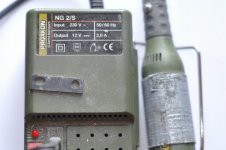
A stove to heat the solution, after wards you can not use that stove for anything else again.
A lot of House hold paper..
A scissor, or sharp knife, and a lot of patience.
Then a good Gram Scale if possible Digital, because all these solutions if you mix them then it's by weight.
And there a gram does matter..
Where
A place where you can rinse the PCB after it has been finished..
Then also a place where you can dispose the used chemicals.
Do not wash it down the drain.
I have 21Pictures to show here. so I need to make 3 parts..
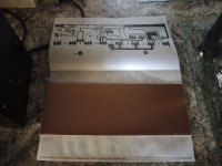
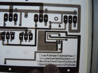
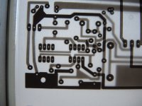
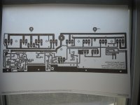
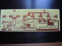
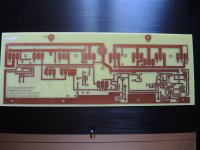
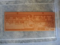
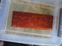
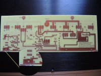
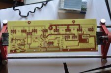
Here, the board I'm going to show, is from today.. PCB is 300x110mm double Sided..
Questions? then just ask.
Some important thing is:
Make sure that the printed side of the Artwork faces the PCB Copper side..
This counts for both the top and the bottom side, that's why it might be necessary that one side of the "Artwork Paper Film" is mirrored.
Usually I mirror the top side.
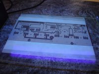
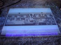
Heat up the ultra violet lamp prior to use for at least 10 minutes, make sure the lamp surface are free of dust or other none welcomed particles..
Make sure the the DEVELOPER Solution does not exceed TEMPS ABOVE 22Degrees Celsius. Neither the container where it is used in. Also check the temp of the PCB must be in the range between 20 & 22 Degrees, if it is higher then put it in the FREEZER until Temp is acceptable.
Using developer below 20 Degrees Celsius, then the film may will not be developed at all or badly, using temps above 23 and more, will give to a fast reaction to the film and the PCB will be unusable.
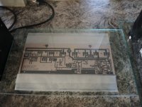
Check out the picture where I align, both sides of the PCB ARTWORK, using a simple Window method. Check out the Pics.
Double sided board must be made in one shot, unless you use to one sided PCB and glue them together..
The most important thing is..
THIS IS THE WAY I DO IT, and It works out that way 99% without failures..
But this does not mean that there are not other ways. I know only that way and may it come handy for the one or the other..
Thanks For reading,
Why:
JMFahey, asked me a while ago to write this,I said yes, and here I keep my promise..
Please Note:
Pictures are numbered so these are self explaining.
Proper Exposing Depending a lot on the BASIS MATERIAL
Testing is easy when using different exposure times, and then check out which one is the best.. therefore a small PCB of square inch or 2.5cm x 2,5cm is enough to find out the right Exposure time..
Proper Developing is not over 2 minutes and that is already long. usually it takes about 50 seconds.
Proper Etching can take up from 5 minutes to 1 Hour depends also on the Solution, the temp of the solution and how much the percentage the mixture contains.
Heating up the solution to 50Degrees will speed up the process quite a lot..
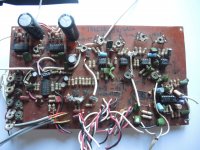
The PCB you see will be the second Prototype of the Variable Current Source Class A Amplifier which will run on Idle up to 2 watts with 0.5AMPERE only
Idle is 0.34 Ampere full load depends on the Load seen at the output. 2Ohms is children play for that AMP.
Thanks to MR. Nelson Pass, for his guidance.. and also Thanks to Mr. Rod Elliot, he, with his version of DOZ was the major Starting Point of this.
Thanks to DIY AUDIO.COM that I can be a member here..
Chris Hess
Here it sends you right away to drilling section
This will bring you direct to assembly Section..
This will bring you to THROUGH HOLE Section
Here a small Guideline Step by Step, how someone could create his own PCB without having a lot of Technical Knowledge, (same as me).
But before we begin here, a few things which come first.
I use BUNGARD Positive Photosensitive PCB's. There are different Manufacturers, but for me, the ones with that light blue protection sheet are the one which, seems to make the least hassles..
Precautions.:
You are working with Chemicals, so protect yourself as good as you can.
Use thin rubber gloves, use if ever possible a separate room.
Do not inhale fumes from developing solution or while etching the PCB from etching solution.
Use Clean environment.
Work in good ventilated rooms or outside on the balcony or where ever you have lots of fresh air.
RTM
Read the manual of the PCB Manufacturer and also read what can go wrong and why it goes wrong, meaning bad and not usable output..
First Comes First: ARTWORK
But first you need to create your artwork, Single side or double side makes actually not a big difference, except that if you want to make double sided PCB, the fact is if you fail on either side you have to throw away the PCB as a whole..
A few word for manufacturing:
Keep in mind that Temperatures of all the components play a big role but also surrounding temp in your room.
For German manufacturers like Bungard, they give a lead of 20 Degrees Celsius, but not over 22 and not UNDER 20 so be exact there.
Tools you need
A Good BEAM Temp Meter where you can be sure that it measure the temp on 0.1 Degree, never mind if this is Water or Ice, Stone, Iron, Aluminum never mind the color the surface has.. ( there are cheap Temp Measuring tools out there, depending on color these will not read the correct temp.
A few plastic containers, to develop and Etch the PCB-.
Thin rubber or silicone Hand gloves.
A Ultra Violet Lamp or Exposing unit. Minimum 40 Watts
A good Paper Cutting Machine where it enables you to also cut PCB's. (check out Picture 1.6)
You need a even Surface which does not bend.
You will also need a two 3 - 5mm thick Glass Plates, large enough to cover the PCB you are going to make.
You need a Timer or Stopwatch.
You will need a certain amount of Film developing solution then also either Sodium per-sulfate. (etching Solution) Ferro chloride II 40 / 60%
A stove to heat the solution, after wards you can not use that stove for anything else again.
A lot of House hold paper..
A scissor, or sharp knife, and a lot of patience.
Then a good Gram Scale if possible Digital, because all these solutions if you mix them then it's by weight.
And there a gram does matter..
Where
A place where you can rinse the PCB after it has been finished..
Then also a place where you can dispose the used chemicals.
Do not wash it down the drain.
I have 21Pictures to show here. so I need to make 3 parts..
Here, the board I'm going to show, is from today.. PCB is 300x110mm double Sided..
Questions? then just ask.
Some important thing is:
Make sure that the printed side of the Artwork faces the PCB Copper side..
This counts for both the top and the bottom side, that's why it might be necessary that one side of the "Artwork Paper Film" is mirrored.
Usually I mirror the top side.
Heat up the ultra violet lamp prior to use for at least 10 minutes, make sure the lamp surface are free of dust or other none welcomed particles..
Make sure the the DEVELOPER Solution does not exceed TEMPS ABOVE 22Degrees Celsius. Neither the container where it is used in. Also check the temp of the PCB must be in the range between 20 & 22 Degrees, if it is higher then put it in the FREEZER until Temp is acceptable.
Using developer below 20 Degrees Celsius, then the film may will not be developed at all or badly, using temps above 23 and more, will give to a fast reaction to the film and the PCB will be unusable.
Check out the picture where I align, both sides of the PCB ARTWORK, using a simple Window method. Check out the Pics.
Double sided board must be made in one shot, unless you use to one sided PCB and glue them together..
The most important thing is..
THIS IS THE WAY I DO IT, and It works out that way 99% without failures..
But this does not mean that there are not other ways. I know only that way and may it come handy for the one or the other..
Thanks For reading,
Why:
JMFahey, asked me a while ago to write this,I said yes, and here I keep my promise..
Please Note:
Pictures are numbered so these are self explaining.
Proper Exposing Depending a lot on the BASIS MATERIAL
Testing is easy when using different exposure times, and then check out which one is the best.. therefore a small PCB of square inch or 2.5cm x 2,5cm is enough to find out the right Exposure time..
Proper Developing is not over 2 minutes and that is already long. usually it takes about 50 seconds.
Proper Etching can take up from 5 minutes to 1 Hour depends also on the Solution, the temp of the solution and how much the percentage the mixture contains.
Heating up the solution to 50Degrees will speed up the process quite a lot..
The PCB you see will be the second Prototype of the Variable Current Source Class A Amplifier which will run on Idle up to 2 watts with 0.5AMPERE only
Idle is 0.34 Ampere full load depends on the Load seen at the output. 2Ohms is children play for that AMP.
Thanks to MR. Nelson Pass, for his guidance.. and also Thanks to Mr. Rod Elliot, he, with his version of DOZ was the major Starting Point of this.
Thanks to DIY AUDIO.COM that I can be a member here..
Chris Hess
Attachments
-
 1. Cutting Artwork.jpg264.6 KB · Views: 399
 -
 1.8. Getting The PCB into Sandwitch between the Artworkt.jpg157.7 KB · Views: 163
 -
 1.7 PCB final size.jpg191.2 KB · Views: 150
 -
 1.6 Measure and Cut PCB to rigth size.jpg186.7 KB · Views: 158
 -
 1.5 Justify Correctness of Vias & Holes right side.jpg165.6 KB · Views: 132
 -
 1.4 Justify Correctness of VIAS & holes.jpg143.2 KB · Views: 126
 -
 1.3 Aligning Artwork Bottom and Top.jpg166.8 KB · Views: 441
 -
 1.2 Top Side Artwork.jpg157.2 KB · Views: 439
 -
 1.1 Bootom Side Artwork.jpg161.2 KB · Views: 459
 -
 1.0 Pre Heating Ultra violet Lamps.jpg198.8 KB · Views: 448
Last edited:
Part Two - Only follow up Pictures
Here the follow up pictures..
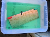
These Red and Black and Green Plastic are to prevents that the surface of the PCB hits the bottom of the Container.
Self explaining.
Here the follow up pictures..
These Red and Black and Green Plastic are to prevents that the surface of the PCB hits the bottom of the Container.
Self explaining.
Attachments
-
 2.8 Top side After Etching ...jpg138.2 KB · Views: 162
 -
 2.7 Bottemside after etching..finished and ready to drill.jpg154.1 KB · Views: 154
 -
 2.6 Start to Etch.jpg128.9 KB · Views: 131
 -
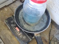 2.5 Heating etching Solution to 50 Degrees.jpg209.4 KB · Views: 181
 -
 2.4 Developing almost finished after 60 Seconds.jpg126.3 KB · Views: 120
 -
 2.3 Developing.jpg123.6 KB · Views: 121
 -
 2.2 Temp Film Developer.jpg87 KB · Views: 111
 -
 2.1 Exposing Top Side for 225 Seconds.jpg162.2 KB · Views: 187
 -
 2. Exposing with Ultraviolet for 225Seconds.jpg178.1 KB · Views: 127
 -
 1.9 Covering the Artwork with Glas Plate...jpg203.8 KB · Views: 158
Part Three - Finishing the job..
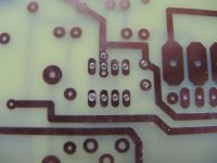
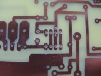
The picture in this post shows both edges of the top side of the PCB looking quite ugly.
This is because the PCB was fixed using duct tape with the Artwork Paper..
but this is of no concern and can be taken care of very easy.
In the meantime I checked the VIAS of the two sides, couldn't be better..
Meaning the holes of top and bottom side matching as it should be..
Thanks for reading..
Chris Hess
Attachments
PCB looks good
Good Day
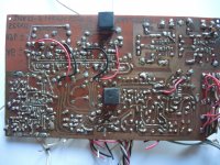
8am something September 6th 2021, controlled the Vias and through pads of that board I made yesterday for accuracy.
So see by yourself. It's quite acceptable for hand drill and hand made, it's withing 0.1 mm or less for a 0.5mm hole. with this I mean not hitting the center of the holes..
Picture 1.0 is from left side of the board, bottom side. Picture 1.1 is from left side Top side of the board the same piece, so we can see that this is QK. to insert the component which in that case is a NE5534 IC used as a PID Regulation, or just call it Servo Control. ( this is pic most left and most right) sorry for that it's because of it's naming.
The same counts for Pictures 2 and 2.1 but residing in the middle. Also made from right side, and all are withing this limits stated above..
This PCB, was done in less than 1 hour time, not including the Artwork, (drawing) but form the moment of printing it out on paper.. till finished PCB Finish meaning Etched..
It will take another 30 minutes to drill it, as this is all made by hand drill..
After that Board will be cleaned and prepared for assembling components.
also Holes on the heat sink will be drilled and threaded..
Enjoy the day and thanks a lot for reading..
Regards
Chris Hess
Good Day
8am something September 6th 2021, controlled the Vias and through pads of that board I made yesterday for accuracy.
So see by yourself. It's quite acceptable for hand drill and hand made, it's withing 0.1 mm or less for a 0.5mm hole. with this I mean not hitting the center of the holes..
Picture 1.0 is from left side of the board, bottom side. Picture 1.1 is from left side Top side of the board the same piece, so we can see that this is QK. to insert the component which in that case is a NE5534 IC used as a PID Regulation, or just call it Servo Control. ( this is pic most left and most right) sorry for that it's because of it's naming.
The same counts for Pictures 2 and 2.1 but residing in the middle. Also made from right side, and all are withing this limits stated above..
This PCB, was done in less than 1 hour time, not including the Artwork, (drawing) but form the moment of printing it out on paper.. till finished PCB Finish meaning Etched..
It will take another 30 minutes to drill it, as this is all made by hand drill..
After that Board will be cleaned and prepared for assembling components.
also Holes on the heat sink will be drilled and threaded..
Enjoy the day and thanks a lot for reading..
Regards
Chris Hess
Attachments
Nice effort.
I made my own PCBs twenty years ago. Laser printer, regular printer paper, lacquered PCBs, put the PCB with printed paper in DIY UV-light box, expose a few minutes, repeat for second side, develop with sodium hydroxide, etch in tank with sodium persulfate (some heating required and a small bubble pump for some circulation). Cut the boards with cheap cutter, drill by hand, install and solder via jumpers. I even tried sandwiched boards once like a thick four-layer board. The result was not always good. It was an experience, at least.
Nowadays it is too easy to send gerber files to jlcpcb, pay $15, wait one week and get fantastic looking boards back that solder easily.
Thanks for your Input it's appreciated.!
About sending Gerber files out:
Then there are some on this site who will NOT consider that as DIY ...If you need examples I can show you some here.. But it's far out /
May some would write a thread when something is to be considered as DIY or Not DIY..
Not my job, I do things and I do not need Authorization of anyone how and why I do something or not..* this is globally spoken nothing wrong with your post.. I like your post.*
When I started out in the 70'ies I used a PEN to draw the PCB lines..
After that a cutter to make the tracks look like tracks, and for the donuts it took quite some time to get them round..
This above is in the status of PROTOTYPE, so I do not want nor need to waste time more than necessary, on a simple PCB Board anyone can do without having experience in making boards.,,
The board you see it has not been processed yet to the real finish of it, because it's only for testing. the final one will look as good as the ones from jlcpcb.. But I understand you and I respect that, what you write..
Bringing up an amplifier where someone copy paste the circuit or the LAYOUT of a PCB or sending in the Gerber files, is easy, not much can go wrong, but as soon someone is into Modifying certain circuits to better or worse don't matter then also there is not a standard, PCB or layout one can use.
As you wrote above, the results are no always good.. but if not then it will be better the next time when better and properly done..
So in fact we think both the same way.. I like to create the whole machine from start to end.. And if it don't work, I'm not too proud to take the blame..
Easy no sweat for me..
One more thing, money was never a concern for me.. otherwise I would stop long time ago, with DIY. for me only one thing count: make it at least as good as the one from the other guys, if possible make it better,
Wait and see the result when this one is finished, may it will take another two or three test boards until I'm satisfied.. No problem.. I like that..
Thanks for your input.. it's always interesting to read what other people like or not. have nice time up there in Finland..
Regards
Chris
Last edited:
Its 40 years since I last did my own pcb.
With the onset of very cheap Chinese pcb makers its a waste of time and effort now.
They also test the pcb so you know there are no shorts or breaks in the tracks.
You get a nice coloured pcb with neat silk screen and tinned pads to stop oxidisation of the copper.
With the onset of very cheap Chinese pcb makers its a waste of time and effort now.
They also test the pcb so you know there are no shorts or breaks in the tracks.
You get a nice coloured pcb with neat silk screen and tinned pads to stop oxidisation of the copper.
I have audio amplifiers and lab meters that I still use that have PCBs that I etched myself. You appreciate things more, the more effort you put into building them. Respect to you, sir, for documenting things.
No Sir please, just use Chris and thank you for the roses..
I think we both are close to each other if it comes to age..
69 this year.. next month
BTW The last time I went back to see relatives in Thailand (2019), a guy brought an Amplifier to me I build in 1992.. Please repair it for me, he asked me..
All what was broken, Solder got old and crappy.. bad contact on Positive terminal.. These PCB Boards I used that time, I had to apply with heating a Photo positive Film and then using 2.5 minutes sunlight to Copy the image on to the film the rest is as you know
Problem was to have that film really good on the Copper layer. using a IRON to get it neat and clean with about 60 degrees Celsius, to hot it would get stiff and break to cold the film would loosen itself from the surface when etching..
Was my best time in my life, 28 years in Thailand at one time and about 2 years with travelling in between....
Thanks Johann and Regards
Chris
Its 40 years since I last did my own pcb.
With the onset of very cheap Chinese pcb makers its a waste of time and effort now.
They also test the pcb so you know there are no shorts or breaks in the tracks.
You get a nice coloured pcb with neat silk screen and tinned pads to stop oxidisation of the copper.
Nigel
I understand you very well, and I know what you mean..
I have traveled China 8 times and if there wouldn't be corona then I would be in china present time..
As soon I get home, I will get some pics online of a PCB I made 1970, drawn by hand.. no corrosion whatsoever..
Manufactured by hand..
This PCB I showed above took me 1 hour to make.. it's much less than 1 Week
And it works, I know how to Gold plate it even it has been etched already.. have done it many times..
You sure know the song of small faces, (Steve Marriot) Lazy Sunday afternoon. So make a fast good looking PCB
The layout anyone has to draw anyways, and one hour later the PCB is finished, this leaves no room for more wishes,,
May if I would sell these but no My amps are not to sell all of them are unique. Max two pieces..
Thanks for your input..
My respect to all
Regards
Chris
Last edited:
Preamp RC4739 build 1981 PCB drawn by hand
@nigelwright7557
Here two Pictures of a Pre Amp, Tone Control, Line drive I build and drew it directly with MAGIC PEN, Staedler it was if I remember right, on to the copper and then used a Art knife to shape the Tracks,.,
This was already beginning of the eighties sometime close to Xmas 1981..
I had done other things in the 70'ies but most of them got lost, when we moved back to Switzerland in 2002.. *If I find them I will place them at a later time..*
and the tracks kept till today and I'm sure that this one still works..
buy good Basis material, don't save the penny on the wrong place, invest something for your peace of heart and it will hold a life time..
Your able to see the date of manufacturing on the RCA Chips number RC4739 which were some of the best OP AMPS that time.. besides the Raytheon there are the numbers 80 36 this means 36th Week of 1980 was manufacturing date of these IC's.. This one run on +- 16 Volts.. Tone control was created with 4 UA741. the 4739 was used to switch the channels bounce less.. it's 40years , long time may I set up power supply to test it..
Regards
Chris Hess
Attachments
Last edited:
ThanksHi Guys
Here a small Guideline Step by Step, how someone could create his own PCB .............
Chris Hess
")
Specially because of the detailed step by step guide and doubly so by the pictures showing it all.
Once you learnt something ... you learnt it, but for a beginner , details who we do not even explain because we consider them "self evident"
... are not so much and often cause doubts.Just reading some questions around clearly show that.
As a side note, we old timers (kind word for "old mummies"
 ) did go through the full DIYing many parts for sheer unavailability of them, or expensive slow procurement, now "you kids have it easy" he he but of course many then have very little practical experience on what I call the "mechanical" side of DIYing, limiting themselves to soldering and assembling using no more than screwdrivers and some Hex key.
 Brave New World , helps a lot, on the other side sometimes it can be limiting
Ordering PCBs for $15 and waiting 1 week to 10 days?
Fine with me, go ahead, but it depends on location.
If outside USA, Canada or Wesern Europe, things can become expensive/complicated and sloooowwww.
Here in Argentina $15 worth of PCBs (excellent price) pays $45 to $65 freight if using DHL-FEdEx-UPS and 10 days, $35-45 + 10-15 days if EMS and all former "cheap Chinese freight/Mail" $15 options have been "temporarily suspended"
for almost 1 year now. So these home made Photopositive methods offer very high definition and very quick turnaround.
As in 1 or 2 hours from screen image to working populated board
More important: rinse and repeat NOW!! if needed
If leisurely building something, no big deal; if prototyping .... invaluable.
Thanks again.
PS: not sure on Bungard but on photopositive boards available here I do NOT remove the remaining cured resist after etching.
I leave it on to protect copper, it looks like a light blue/greenish "solder mask" and no need to remove it from pads for soldering, on cntact with molten solder it melts/evaporates away in a manner very similar to "self soldering enamel" used in some types of magnet wire.
Not sure if on purpose or by sheer chance, but that´s an added bonus.
Last edited:
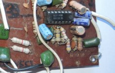
Some special from the manufacturer- to keep the board nice
Yes, I do that too. Leaving the Film as protective layer unless I'm going to gold plate it, then just scraping of the Donuts is no option the Board has to be cleaned and afterwards wiped.. This as far I know, was made on purpose to protect the board by Bungard.. and the fortune of it, it can be soldered without leaving dirt or burned leftovers.
It also depends how bad it is scratched when soldering the Components into..
The shielding Bungard uses is golden brown as you can see in the pictures.
It does protect the board very well, indeed.
If I need to remove that protective layer then, to secure the board I have special mixture. taking a few grams Tree sap and mixing it with 50 - 100 ml thinner * nitro thinner not Synthetic resin * then use an old piece of cloth and dump in that solution and gently wipe the board with it.. this will dry instantly, is protecting the board and also no need to wipe off in the case that there is need to solder on the board.
Regards
Chris Hess
Please link to it, I bet it will also be useful.Well I mean I have a wiki article on this but more guides are always a good thing.
About Drilling
I will extend this guide to the next step =
Drilling
After that I will extend the thread to the next step
And this will be
Assembling
Then the next step will be
Controlling
and the last will be
Testing
All these steps will be available from the 1st Page..
May we can give some hand to the ones who are in need of
Drilling will be up today...
Regards
Chris Hess
Drilling is a problem by itself.
Regular steel drills are fine, but last little if glass fiber is present.
Of course they are cheap, so you buy a pack of 1mm (easy) or 0.85mm (not that much) and consider them a somewhat disposable item.
No big deal for home builders.
You can buy dedicated "PCB drills" with a uniform mounting base and Tungsten Carbide (Widia) tips
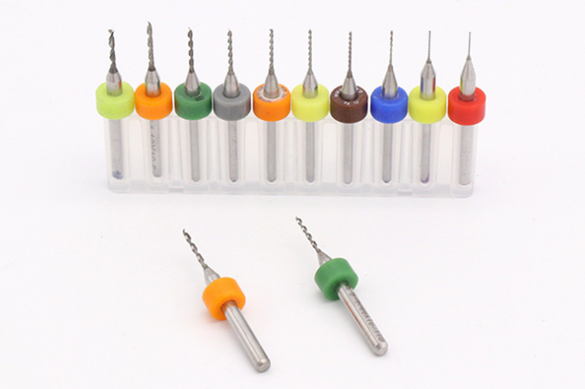
BUT, and that is a problem at home, requires a special drill press, both very high RPM and, most important, ZERO chuck vibration, they are very fragile.
Counterintuitively, mounting them in a handheld Dremel type tool damps vibrations and is relatively safe.
Regular steel drills are fine, but last little if glass fiber is present.
Of course they are cheap, so you buy a pack of 1mm (easy) or 0.85mm (not that much) and consider them a somewhat disposable item.
No big deal for home builders.
You can buy dedicated "PCB drills" with a uniform mounting base and Tungsten Carbide (Widia) tips
BUT, and that is a problem at home, requires a special drill press, both very high RPM and, most important, ZERO chuck vibration, they are very fragile.
Counterintuitively, mounting them in a handheld Dremel type tool damps vibrations and is relatively safe.
This here is my Bungard process.
I make my boards usually single sided + GND
That makes top & bottom alignment easy / unnecessary.
< 1__layout | Gerhard Hoffmann | Flickr >
+ the some pics to the right.
Yes, I know JLCPCB. I just got 3 different designs from then 2 weeks ago.
But my process is 2 hours from artwork in the computer to soldering.
Please link to it, I bet it will also be useful.
I mean it's supposed to be easy to find.
PCB fabrication.
About Drilling
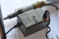
FAGILE Yes, but easy to hand drillif one has a steady hand.. I very seldom break a drill using a Proxxon Dremel.. drilling with exactly these drills starting at 0.mm (this fits IC pins..) then 0.8 and go on to 0.8mm and then 1.2mm - 2mm and 3 mm for the screws. 6mm for holes to tighten Transistor Screws passing the screwdriver (inside Imbus HEX) through to PCB..
I use also that PCB holder to fix the PCB while drilling..
I also have a drilling Stand.
I'm in a hurry get back later..
Chris
Drilling is a problem by itself.
You can buy dedicated "PCB drills" with a uniform mounting base and Tungsten Carbide (Widia) tips
BUT, and that is a problem at home, requires a special drill press, both very high RPM and, most important, ZERO chuck vibration, they are very fragile.
Counterintuitively, mounting them in a handheld Dremel type tool damps vibrations and is relatively safe.
FAGILE Yes, but easy to hand drillif one has a steady hand.. I very seldom break a drill using a Proxxon Dremel.. drilling with exactly these drills starting at 0.mm (this fits IC pins..) then 0.8 and go on to 0.8mm and then 1.2mm - 2mm and 3 mm for the screws. 6mm for holes to tighten Transistor Screws passing the screwdriver (inside Imbus HEX) through to PCB..
I use also that PCB holder to fix the PCB while drilling..
I also have a drilling Stand.
I'm in a hurry get back later..
Chris
Attachments
- Home
- Design & Build
- Construction Tips
- Making a double Sided PCB Guide - how it could be done..