Hi
Just to make it clear, this Circuit consist alot of a schematic drawn by or designed by Rod Elliot, and also some Parts where Nelson Pass plays a Big role in it, when he helped me out to correct my thinking of many different calculations, with the test Program I use.,
His major speech to me was something like that..
"I'm interested in the real world Amplifier more than simulations" and of course he is right, he's Nelson Pass, the Master of Amplifiers.
Also he showed me the shortcomings, of the last build of mine.. In fact it isn't a shortcoming for me because I designed the Amplifier as it is today, and it turned out better than I expected. The Single End Class A Amplifier from one of my last threads. But there is no playground if it comes to professional Designers and Builders as Nelson Pass and Rod Elliot are. the all has to be by the book. I dreamed of 25 Watts, I got over 30@8 Ohm with THD of less than .5% and less than .05% @1 Watt RMS in my last build..
Of which I have to say that this one just works like a dream and Charm and it sounds real good. Natural...
Mr. Nelson Pass was it, who wrote to me, that using RE a 250 Watts Resistor would lose too much power compared to Power Consumption, and this is TRUE (this in my last build) and that it would be better to stick with Constant Current Source for the Class A. But the levels I listen too are in the range up to max 5 Watts, anything else is just too loud.
But Constant Current Source Class A Amps, I had already done 2013 / 2017 which has again grown out of a design from Rod Elliot DoZ circuit, but which was completely modified by myself. I had sent the modifications to Rod Eliot by email that time, so he knows about this. And this here is the EXTENSION 2021 with some modification compared to that 2 Constant Current Source Class A Amps, I build in 2013 and 2017 respectively, both which are in best condition till today..
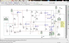
Now the circuit you see I added is a Mix of all these Inputs I've got from Nelson Pass as well as from Rod Elliot's designs and from other sources, many thoughts, I read here, I try to implement here.
I call it Variable Current Class A Amplifier, even I know that there is no VARIABLE CURRENT if it's Class A.
In fact, Adding one more resistor and adding a simple three pole switch can turn this amplifier into a CONSTANT CURRENT SOURCE CLASS A in no time and it can be freely adjusted beginning at 200Milli-amps up to 20 Ampere Idle
The reason to do this (Variable Current Source) is, I try to handle the current when there is no signal on the OUTPUT Transistors, that it will be around 500 / 750 Milli-amp while IDLE but will get full Current on Full Load. So may I can help the ICE BEARS, that the White Gold for them *ICE in the Arktis* will stay somewhat longer..
But I'm not really sure if this still fits into Class A.. that's why here again my Question,
What Class Would YOU put this AMPLIFIER into.??
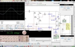
BTW this amp is working on my Bench as you can see it in the Schematic, here.. it has a few add-ons to compensate heat and to keep Super 0.0000Volts at the output at anytime while running.
Right now I'm drawing the Artwork, or call it layout for large Heat Sinks, 400mm X 150mm X 100mm.
The Design *Simulations* showing 3 versions you can have the read out in that yellow window, once with no SIGNAL at the input but Amp is running idle, and once with 1Khz under Full Load driven into 4 Ohms and then also driven into 8 Ohms and also with Signal switched off.
This way class a could be suitable while in IDLE State, using a mere of 18 Watts while in Idle *depends how high Bias is set too*, about 30 Watts up to 10 watts output and 180 Watt for full output Power. Can this still be considered as CLASS A? More follow soon.
Thanks for any Input.
Regards Chris Hess
Just to make it clear, this Circuit consist alot of a schematic drawn by or designed by Rod Elliot, and also some Parts where Nelson Pass plays a Big role in it, when he helped me out to correct my thinking of many different calculations, with the test Program I use.,
His major speech to me was something like that..
"I'm interested in the real world Amplifier more than simulations" and of course he is right, he's Nelson Pass, the Master of Amplifiers.
Also he showed me the shortcomings, of the last build of mine.. In fact it isn't a shortcoming for me because I designed the Amplifier as it is today, and it turned out better than I expected. The Single End Class A Amplifier from one of my last threads. But there is no playground if it comes to professional Designers and Builders as Nelson Pass and Rod Elliot are. the all has to be by the book. I dreamed of 25 Watts, I got over 30@8 Ohm with THD of less than .5% and less than .05% @1 Watt RMS in my last build..
Of which I have to say that this one just works like a dream and Charm and it sounds real good. Natural...
Mr. Nelson Pass was it, who wrote to me, that using RE a 250 Watts Resistor would lose too much power compared to Power Consumption, and this is TRUE (this in my last build) and that it would be better to stick with Constant Current Source for the Class A. But the levels I listen too are in the range up to max 5 Watts, anything else is just too loud.
But Constant Current Source Class A Amps, I had already done 2013 / 2017 which has again grown out of a design from Rod Elliot DoZ circuit, but which was completely modified by myself. I had sent the modifications to Rod Eliot by email that time, so he knows about this. And this here is the EXTENSION 2021 with some modification compared to that 2 Constant Current Source Class A Amps, I build in 2013 and 2017 respectively, both which are in best condition till today..
Now the circuit you see I added is a Mix of all these Inputs I've got from Nelson Pass as well as from Rod Elliot's designs and from other sources, many thoughts, I read here, I try to implement here.
I call it Variable Current Class A Amplifier, even I know that there is no VARIABLE CURRENT if it's Class A.
In fact, Adding one more resistor and adding a simple three pole switch can turn this amplifier into a CONSTANT CURRENT SOURCE CLASS A in no time and it can be freely adjusted beginning at 200Milli-amps up to 20 Ampere Idle
The reason to do this (Variable Current Source) is, I try to handle the current when there is no signal on the OUTPUT Transistors, that it will be around 500 / 750 Milli-amp while IDLE but will get full Current on Full Load. So may I can help the ICE BEARS, that the White Gold for them *ICE in the Arktis* will stay somewhat longer..
But I'm not really sure if this still fits into Class A.. that's why here again my Question,
What Class Would YOU put this AMPLIFIER into.??
BTW this amp is working on my Bench as you can see it in the Schematic, here.. it has a few add-ons to compensate heat and to keep Super 0.0000Volts at the output at anytime while running.
Right now I'm drawing the Artwork, or call it layout for large Heat Sinks, 400mm X 150mm X 100mm.
The Design *Simulations* showing 3 versions you can have the read out in that yellow window, once with no SIGNAL at the input but Amp is running idle, and once with 1Khz under Full Load driven into 4 Ohms and then also driven into 8 Ohms and also with Signal switched off.
This way class a could be suitable while in IDLE State, using a mere of 18 Watts while in Idle *depends how high Bias is set too*, about 30 Watts up to 10 watts output and 180 Watt for full output Power. Can this still be considered as CLASS A? More follow soon.
Thanks for any Input.
Regards Chris Hess
Attachments
-
 1. Class A - No signal 8 Ohm.jpg178.1 KB · Views: 657
 -
 2. Class A - Full Load 8 Ohm.jpg177.7 KB · Views: 645
 -
 3. Class A - No Signal 8 Ohms.jpg189 KB · Views: 601
 -
 3. Class A - Full load 8Ohm.jpg205.2 KB · Views: 567
 -
 5. Class A - Idla No Signal 4 Ohms.jpg200.5 KB · Views: 558
 -
 4. Class A - Full Load 4 Ohms.jpg205.5 KB · Views: 185
Last edited:
Thank you for your input
NO always on.
What you want to know else, I'm open for everything.
We can remove Q 5& 6 and the amp will still work with a few milli-watt
Q5 Q6 are Current Source.
Q7 Q8 are paralell for the signal output.
NO always on.
What you want to know else, I'm open for everything.
We can remove Q 5& 6 and the amp will still work with a few milli-watt
Q5 Q6 are Current Source.
Q7 Q8 are paralell for the signal output.
Attachments
Last edited:
Input *Q1 & VRB adjusting DC OUTPUT was desinged by Rod Elliot, But with Single Rail only and no DC Lock on the the Base of Q1.
Q2, I implmented just as a Impedance Changer and Buffer for Q1.
When Q2 is not used that way, Hum will Noise will be increased by at least 60DB and Hum inclusive Noise will be audible, when Speakers are connected.. even it's only a few milli volts. but it's audible.
Q3 is Current Source driver for Q5 Q6 can be adjusted to prevent positive wave clipping, adjusting too much, will increase IDLE CURRENT.
Q4 is Signal driver for Q7 Q8 where R4 can be used to adjust over all IDLE CURRENT changing this resistor to 5Ohm, then IDLE will be 17AMPS
Amp has a bandwidth 10Hz - 100Khz -2db @100Khz
Amp can be run with 8Ohms @2.5 Ampere are 64 Watts output, with less than 0.3% distortion
Anything you want to know guys I will answer.,, this Amp will not use any FANS for COOLING. Large Heatsinks instead.
Attachments
In the design there are only 4 transistors drawn.
In reality there are all together 10.
5 for the current Source and five for Signal output
Not using Balast resistors on Emitter of the Current Source will heatup the Transistor very differently as much as 10 - 15 degrees compared to the other Transistors. Even transistors are mounted on a large heat Sink, as you have seen in my last picture.
Measuring the Transistors HFE GAIN first will help to reduce the heat but these resistors will help to dissipate the heat more evenly.
The same is with the Signals transistors Q7 Q8..
Just to make sure that Heat dissipates evenly, and if I place them also in Emitter distortion measures are higher..
And do not forget in the endproduct there will be 5 Transistors which generating heat, and 5 transitors which must work together as ONE* not only formula 1* here as well. So thats the countermeasure I take to cope with heat problems out of not exactly the same GAIN of transistor.
Lately someone very smart told me: The simulators work quite well – it’s the quality of the transistor models that usually falls short.
And I'm sure that this is exactly that way, If I use only 2 Transistors per Current Source and another 2 for the Signal part then there is no need for these Balast Resistors.. but with 5 then there is a need.
Before I started to do this, I always had problems, that Transistors would differ very much when measured the HEAT on the Transistor BODY. Now I have them down to say 1- 2 degress difference.
Anything wrong with it, or do you have a better option way to solve the problem. I'm eager to know. Only that way this amp will work as expected.!
I can assure you that I take maximum Care in this matter. In the past I had to reduce IDLE CURRENT on one of my builds, because heat always broke one of the transistors. Then I tried to use a Trasistor with less HFE GAIN in that place, so it worked but, then the another transistor would heat up. So after alot of of reading was this the way and the solution I found.
Actually, the resistors should be calculated for each transistor, so that it would affect on that part where the transistor runs off when heating. But this is very much testing, and very time consuming. If I reduce HFE GAIN, sound isn't as good as I want.
I buy 50 MJL4281 to get 10 transistors with the same HFE. Most times it works that way sometimes it don't. the rest of the transistors I use for testing.
And it sure makes a big difference in sound, in responce, in linearity when parallel them in two block with same HFE GAIN and same heat. these Resistors are adding only 0.01% distortion, so never mind. I can live with that.
That AMP I build last year, uses +- 40 Volts Rail Voltages with RE 7.5 Ohms /250 Watts *NO CURRENT SOURCE TRANSISTOR*
So Idle current is from the time the switch is flipped just 5 Ampere. and not 5.3 because, even I use 750VA Transformers, 30 - 0 - 30 @12.5 Ampere voltage drops down to 37.5volt DC..and all I get out is about 28.125 Watts RMS@8 Ohms in best case with a distortion below of 0.3 % over the full Bandwidth or 15Volts RMS
Which is equal to 28 Watts
But that amp I created last year can handle Loads of 1.5 Ohms and will be ables to deliver Peak to Peak 29Volts @ 1.5 Ohms Before Clipping and this in REAL TIME. 69 Watts RMS
This amp here delivers twice as much, with less Current.
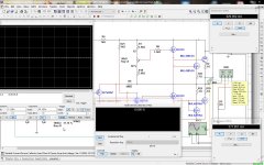
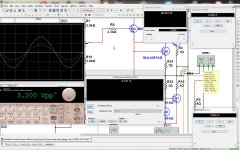
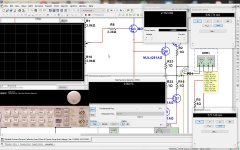
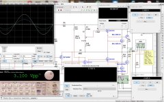
Again, do you or anyone else think that this is still Class A? Check out the picture..My Goal is it to use only as much Current as the Speaker is requesting to deliver a clean sound, and with this circuit this is possible..
So not too much "waste" which just heats my house up..
Because as soon I reduce the Volume, also current draw will be reduces which is at 1WATT *check out the picture* 0.45Amps.
I hope that I was able to answer your question and also this is the way I understand it.
But as you can see in Picture with that 1 Watt Response, distortion is up and more than with full output, but this will be adjusted finally when the PCB are made and screwed and the board is screwed to heat sinks, then it should be in the range of 0.09% or similar. More current = less distortion. Question is how much is enough.
If this is not correct, please let me know now, because it could save me a lot of time while designing the PCB, which I'm working on rigth now. Pic, PCB is not finished yet. double sided. test PCB with 4 Transistor I already have, vut there were some major parts not the way as expected. But the most important thing, that Variable Current Source is working.
Thanks everyone here.
My english is too bad to explain it all so everyone understand what I mean.
Regards Chris Hess
In reality there are all together 10.
5 for the current Source and five for Signal output
Not using Balast resistors on Emitter of the Current Source will heatup the Transistor very differently as much as 10 - 15 degrees compared to the other Transistors. Even transistors are mounted on a large heat Sink, as you have seen in my last picture.
Measuring the Transistors HFE GAIN first will help to reduce the heat but these resistors will help to dissipate the heat more evenly.
The same is with the Signals transistors Q7 Q8..
Just to make sure that Heat dissipates evenly, and if I place them also in Emitter distortion measures are higher..
And do not forget in the endproduct there will be 5 Transistors which generating heat, and 5 transitors which must work together as ONE* not only formula 1* here as well. So thats the countermeasure I take to cope with heat problems out of not exactly the same GAIN of transistor.
Lately someone very smart told me: The simulators work quite well – it’s the quality of the transistor models that usually falls short.
And I'm sure that this is exactly that way, If I use only 2 Transistors per Current Source and another 2 for the Signal part then there is no need for these Balast Resistors.. but with 5 then there is a need.
Before I started to do this, I always had problems, that Transistors would differ very much when measured the HEAT on the Transistor BODY. Now I have them down to say 1- 2 degress difference.
Anything wrong with it, or do you have a better option way to solve the problem. I'm eager to know. Only that way this amp will work as expected.!
I can assure you that I take maximum Care in this matter. In the past I had to reduce IDLE CURRENT on one of my builds, because heat always broke one of the transistors. Then I tried to use a Trasistor with less HFE GAIN in that place, so it worked but, then the another transistor would heat up. So after alot of of reading was this the way and the solution I found.
Actually, the resistors should be calculated for each transistor, so that it would affect on that part where the transistor runs off when heating. But this is very much testing, and very time consuming. If I reduce HFE GAIN, sound isn't as good as I want.
I buy 50 MJL4281 to get 10 transistors with the same HFE. Most times it works that way sometimes it don't. the rest of the transistors I use for testing.
And it sure makes a big difference in sound, in responce, in linearity when parallel them in two block with same HFE GAIN and same heat. these Resistors are adding only 0.01% distortion, so never mind. I can live with that.
That AMP I build last year, uses +- 40 Volts Rail Voltages with RE 7.5 Ohms /250 Watts *NO CURRENT SOURCE TRANSISTOR*
So Idle current is from the time the switch is flipped just 5 Ampere. and not 5.3 because, even I use 750VA Transformers, 30 - 0 - 30 @12.5 Ampere voltage drops down to 37.5volt DC..and all I get out is about 28.125 Watts RMS@8 Ohms in best case with a distortion below of 0.3 % over the full Bandwidth or 15Volts RMS
Which is equal to 28 Watts
But that amp I created last year can handle Loads of 1.5 Ohms and will be ables to deliver Peak to Peak 29Volts @ 1.5 Ohms Before Clipping and this in REAL TIME. 69 Watts RMS
This amp here delivers twice as much, with less Current.
Again, do you or anyone else think that this is still Class A? Check out the picture..My Goal is it to use only as much Current as the Speaker is requesting to deliver a clean sound, and with this circuit this is possible..
So not too much "waste" which just heats my house up..
Because as soon I reduce the Volume, also current draw will be reduces which is at 1WATT *check out the picture* 0.45Amps.
I hope that I was able to answer your question and also this is the way I understand it.
But as you can see in Picture with that 1 Watt Response, distortion is up and more than with full output, but this will be adjusted finally when the PCB are made and screwed and the board is screwed to heat sinks, then it should be in the range of 0.09% or similar. More current = less distortion. Question is how much is enough.
If this is not correct, please let me know now, because it could save me a lot of time while designing the PCB, which I'm working on rigth now. Pic, PCB is not finished yet. double sided. test PCB with 4 Transistor I already have, vut there were some major parts not the way as expected. But the most important thing, that Variable Current Source is working.
Thanks everyone here.
My english is too bad to explain it all so everyone understand what I mean.
Regards Chris Hess
Attachments


Last edited:
Hi
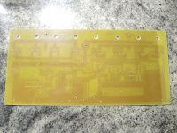
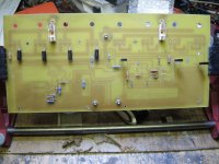
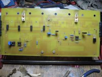
The Layout of the PCB for that Amp - I call it Varaible Class A Current Source I have drawn and rechecked with the Circuit already has been finished..
Now on the left side of the Board I intent to also add a Control unit like SERVO CONTROL, even the AMPLIFIER would work without, then also a control to switch the AMP into CONSTANT CURRENT SOURCE CLASS A AMP - Also a part where the BIAS can be preset from Outside of the Amplifier Chassis, so when finished and all is in the box, it will be easy to adjust different BIASES, to check where the sound is best and for the other part, where the amp uses the least Power Consumption with best sound..
Then also a Control with lots of BIAS on LOW VOLTAGE, of course all this within the means of possibility.
As you can see in the picture I placed, the PCB is 395mm Long (15.5 Inches x 5.5 Inches) and 140mm wide and it is doublesided, so I need to order the PCB first, because I do not have PCB's that large here at home.
Will take a few days, but there is work enough, in the meantime I will make the CHASSIS Ready, and as all my recent amps, it will be an Old MAC PRO Case. Modified.. Only that this one will need more work than usual..
Thanks for reading.
Regards
Chris
Attachments
Last edited:
Low value ballast resistor on Emitters help even out current, make matching much less critical and mke circuit more thermally stable.
In series with collectors, they are only wasting power as heat, with no benefit whatsoever.
I´m talking R22-R10 in series with Q7-Q8 collectors
R23-R2 in series with Q5-Q6 emitters are fine and doing their job.
EDIT: I think you are trying to make a "Sliding Class A" amplifier.
Some Japanese maker made a few in the late 70´s (was it Kenwood???) but they were symmetrical push pull with signal variable Bias; the single ended type you are making was patented in 1961:
US3166719A - Transistorized sliding class a amplifier
- Google Patents
Last edited:
You might be right about the resistor for Q7 Q8, if this would be only two Transistors then there would not be any need to install these R in series, with Collector..
Now in this case, here If I do not install them with 5 Transistors then I run into problems with the matching.
Did you note the I using Quasi Complimentary all are NPN. And Q7 Q8 are amplifying the signal. I have tried both, installing the Resistors at VRail -40 in series with Emitter of Q7 Q8, it turns out that then Distortion goes quite up into the sky and also matching does become critical..
But I'm going to try your thoughts on this one more time.
What would you Do? installing them on Emitter side of Q7 Q8?
I have build that in 2013 and 2017 already but there I run into problem that it was very difficult to take care of the heat, even use very large heat sinks, in both these amps..
Now here I spent a long time to with testing, so I can reduce Idle when there is no signal input but with the output transistor still always on. and then it will increase while signal is increasing, this is actually my goal.
I haven't seen that Patent nor the Amp,from Japan*Kenwood* and the Amp does not look similar.
Also I did not get the inpiration to build from that link but from reading Rod Elliots site.
Reading about DoZ. And also it's the first time that I hear about Sliding Class A.
But many thanks, I'm always open for everything.
Even the single ended version was patented in 1961, I think as similarities are far, I still can build that.. Or??
In not too long time the PCB will be finished and then I can compare and make further tests to find out how good it is. The test version which is on my bench, is fascinating,
and if the sound matches the single End from last year or may even surpassed then I can be satisfied, but still CREDIT goes to two men.. Rod Elliot as well as Nelson Pass. both of them were really helpful, and both of them did not had any reason to help. But both did.
And therefor a Big thank you to you guys. Nelson & Rod.
You guys know how to make people happy.
Last edited:
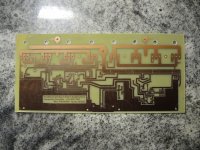
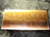
Update on Layout
So, Layout of PCB has been finished only to know that I had to resize it down to 300mm, because double sided PCB is too expensive here, when buying Bungards double Side PCB.
So there is now a 10 Transistor (Output) and a 8 Transistor version.
10 transistor version is 395mm long and 140mm wide.,
The 8 Transistor Version is 300 mm long (actual Tracks length is 295) and 140 wide..But heat sink is still 400mm in length.
Hope to be able to make the PCB today afternoon and then assembling the Amp on Sunday, this of course will include testing. REAL TIME.
The picture shows the 8 transistor version.
Here it's Friday, July 30th. 2021 08:20 in the morning and I will be off to work in a few minutes..
Of course this afternoon after returning from work, I will give the layout a final check, just to be sure to have all tracks connected as this should be.
Till then, guys, enjoy life..
Regards
Chris
Attachments
Last edited:
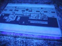
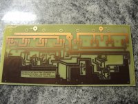
PCB for the drain..
So, I finally made that double sided PCB last night, but it just turned out very UGLY.. LOL
I don't think that it was a problem of the material, rather a problem of myself using too old Film developer..
Part two of that is, because of this I and the situation that I do not have any good double sided Positive Film PCB, and I want to test that AMP Tomorrow, there was no way around for me than Redraw that PCB in Single Side Mode one more time..
Look a the picture.. I have high quality PCB with positive Film from Bungard.
So I will make that board tonight after Work, with the hope that I do not mess it up again.
May it's enough time to finish that amp till tomorrow evening, . Meaning making the PCB, assembling and testing it.. out of the box of course..
Attachments
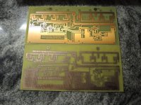
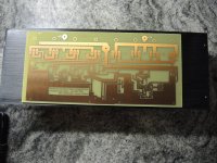
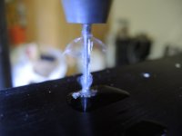
This time PCB - Good.
As promised a few hours ago, I made the PCB, Single sided, but never mind for Testing it's still good enough. and it too only 2 wire Jumps.
Pics are from Exposure to finish drill. Picture number 5 is to compare the PCB from yesterday evening and this one from this evening.
If no big hiccups occur then this Amp will work tomorrow evening. for testing and may have to redraw it, but I'm positive, that it works as expected.
The final version will be of course double side.. as soon I get the new PCB's. Takes a few days or may a week.
I asked Mr. Pass the same question as I do here in this thread..
His answer was like that: Class A, Single End.
According to Mr. Pass - It's also named SEPP = Single End Push Pull and also SRPP = Shunt Regulated Push Pull.
I think for me Variable Current Source Class A Single End, sounds well.
He also wrote that he made many of them. with big success.
Hope that I will be just a tiny bit as successful for this amp as he was.
Again this design was born because of Mr. Nelson Pass and also Rod Elliot,
with modification of some of their circuits amps. So all CREDIT goes to these two.
May we all can find a way to listen to the superior sound of class A but still do not need to sell our house for paying electricity Bills... LOL
The coming days we will know. Idle current for 8 Ohms is 600ma. and this with 40Volts Rail, will be 24 Watts IDLE only for a Class A up to 2 watts, which should have a max output Power RMS of 64WATTS @8ohms.. and will draw 2.6Amps at full load, but this any AB does at well or even more.
Again I like to express my Thanks to everybody here also.
And
Thanks for reading.
Regards and have a nice Weekend
Chris Hess
Attachments
-
 1. Exposing UV_s.jpg170.3 KB · Views: 155
 -
 7. drilled_s.jpg179.2 KB · Views: 70
 -
 6. drilled_s.jpg261.9 KB · Views: 72
 -
 5. Compare with the one from last night_s.jpg257.3 KB · Views: 67
 -
 4. with heat sink_s.jpg223.6 KB · Views: 136
 -
 3. Etched_s.jpg237.5 KB · Views: 137
 -
 2. Developed_s.jpg191.8 KB · Views: 157
Last edited:
Hey! Congratulations! It turned out perfect!!!
Are you using Photopositive boards?
I see you are using Vellum (Architect´s tracing paper)
I also used it a lot , bought a 100 sheet pack over 10 years ago (I silkscreen boards, front panels and cabinet Logotypes) and still have a lot left over but problem is that Laser toner both has tiny pesky pinholes and is denser on edges but thin inside large areas (an electrostatic problem?) so it makes exposure quite critical.
And Vellum slightly expands and contracts depending on ambient humidity, now I pre dry it both before printing and before exposure for consistency.
No big deal for single face boards but shows slight misalignment on double face ones.
Now I exclusively use Polyester film , perfect stability, I print two copies and superimpose them, combined blackness is as good as that of Graphic Arts Litho film, what I used for decades before these fancy Computers and Laser Printers were invented.")
WAY less critical and I avoid the slightly corroded surface you show on one of them.
I have déjá vu with those boards, didn´t you show an earlier version here 1 or 2 yeas ago?
Are you using Photopositive boards?
I see you are using Vellum (Architect´s tracing paper)
I also used it a lot , bought a 100 sheet pack over 10 years ago (I silkscreen boards, front panels and cabinet Logotypes) and still have a lot left over but problem is that Laser toner both has tiny pesky pinholes and is denser on edges but thin inside large areas (an electrostatic problem?) so it makes exposure quite critical.
And Vellum slightly expands and contracts depending on ambient humidity, now I pre dry it both before printing and before exposure for consistency.
No big deal for single face boards but shows slight misalignment on double face ones.
Now I exclusively use Polyester film , perfect stability, I print two copies and superimpose them, combined blackness is as good as that of Graphic Arts Litho film, what I used for decades before these fancy Computers and Laser Printers were invented.
WAY less critical and I avoid the slightly corroded surface you show on one of them.
I have déjá vu with those boards, didn´t you show an earlier version here 1 or 2 yeas ago?
EDIT:tell us something about the Photosensitive material you used , your light source and maybe some details about time, distance, development,etc.
I am certain it will help others.
In fact you might (hint hint ) write a short how-to and upload it into the construction tips section.
I am certain it will help others.
In fact you might (hint hint
) write a short how-to and upload it into the construction tips section.Yes I use Bungard PhotosensitiveHey! Congratulations! It turned out perfect!!!
Are you using Photopositive boards?
I got three blocks of them A4. Each 100 sheets. Very useful. No problems, neither with single or double side.I see you are using Vellum (Architect´s tracing paper)
No, I just drew that board within the last week.. mostly yesterday and today.I have déjá vu with those boards, didn´t you show an earlier version here 1 or 2 yeas ago?
It's brand new. I had a similar one but never showed here.. Check out the date on the board, and the version number that's the drawing I made until I then finally made the board.. so it took me at least 20 hours to complete.. saving them each time with a new number so i could cross check..back.
The one I showed is completely different. it's hosting 6 Transistors but on a area of only 17Cm to 15cm, this board is 30cm to 14cm. But you know a PCB made DIY is like a FINGERPRINT, it's the way someone designs the layout, and you can rely on that.. I have my way how I think it would look right, and therefor the results will look similar,.
Oh BTW, you were right about the Collector Resistors in my Circuit... I messed up, But no harm done there. Simulation Program showed me massive distortion, but afterwards I was talking to Mr. Pass, and he confirmed your doubts about the collector resistors, not in the same way, but that for the reason I would use them only Emitter was to use. So I just moved them to emitter without any problem.
Now, I think for the double sided PCB from yesterday which was a real mess, it was two things which made it happen that it turned out so badly as you can see in the picture.
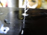
First the Basis Material, was not Bungard and I checked after that the leftover and saw that the cover plastic was not firm tight with the surface of the PCB anymore.
Secondly: I used to old developer.
So I print my artwork with a OKI 5550 Laser, on to the Vellum paper.
The printed side face down to the PCB,
Then a heavy 4mm thick Glass plate.
in a distance of 15 cm above I use two 40 watts ultraviolet lamps and expose it 3minutes 45 seconds to 4 minutes if I use thin lines. Before using the lamps, heat them up for at least 5 - 10 minutes that the shines is thick, cold lamps will not cover that good and the do flicker to much when cold. Lamp is NEON ULTRA VIOLET
You remember last year I went trough hell with making PCB for one month or two and I didn't know what had happen. It was the SUMMER HEAT, Even I measure temps, but I did not measure the temp of the PCB then and these had more then30Degrees Celsius.. it took me quite some time to find out..
Now I check all the temps, prior to making PCB, if too hot I put them into the freezer till I get these 20 degrees, same for the developer solution.
Hope to answer your questions..
Anything you want to know, anyone, just ask.
Last edited:
EDIT:tell us something about the Photosensitive material you used , your light source and maybe some details about time, distance, development,etc.
I am certain it will help others.
In fact you might (hint hint
Yea I will do that. but I need to finish other things before.. next week some time..
And believe me, there are so many factors, you know very well.
and it's not sure that it work for all the same.
But anyway I wills start a thread next week about that. with picture and may a small Video..
That's OK. for you?
Oh, it´s not me specifically, but you were successful and it´s useful to many if you post a short "How To".
Same as happened to you the first time (and to me and to almost everybody else), there´s a lot of seemingly unimportant details (include checking ambient temperature into that) that are neither explainded in Datasheets nor self-evident .
Practice makes perfect, like with everything, but warning of potential obstacles helps a lot.
Thanks.
Swiss National Day, a day to enjoy..
Guys good evening for all in Europe. Good night the ones in Asia and good morning the guys from USA ad the whole west.
Just to make it clear, amp isn't finished, Reason, I broke my Glasses on Friday morning and now using my spare glasses which are from 2007.. Lol.
So it's rather hard to get that amp assembled in the same time. I see only 75% of what I wish to see..
Anyway, I started out to drill the wholes and cut the threads into the heat sink and then I saw that this 3mm Thread Drill or cutter is worn out.
I have a Garage, but this garage is about 65Km from my home, and I got there some thread cutter, but I was to lonely to drive down and get one..
Hey, it's Swiss National Day.. So I decided to assemble the board.
It took me 3 times as long as it would be usual, and my eyes hurt because the glasses aren't strong enough .
Anyway I could assemble some of the components, the rest I will do tomorrow, and if necessary after tomorrow, then I should also get my new Glasses..
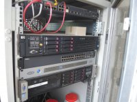
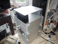
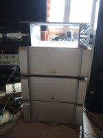
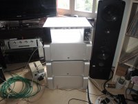
Anyway made some pics,. of that all from today. BTW there is also on of my Server Rack,,which resides on the balcony of our house..
Then also as the heat sink do not have the same height as the other amps you can see in the pics, I need to take measurements to have it look good. check out the pics..
The amp in the middle is named the unfinished one, actually it is finished except the side panels, don't fit because of these fans, I mounted,.. and that way the amp survives the heat. and i can live with that..
That's it..
Be back later time..
Regards Chris
Guys good evening for all in Europe. Good night the ones in Asia and good morning the guys from USA ad the whole west.
Just to make it clear, amp isn't finished, Reason, I broke my Glasses on Friday morning and now using my spare glasses which are from 2007.. Lol.
So it's rather hard to get that amp assembled in the same time. I see only 75% of what I wish to see..
Anyway, I started out to drill the wholes and cut the threads into the heat sink and then I saw that this 3mm Thread Drill or cutter is worn out.
I have a Garage, but this garage is about 65Km from my home, and I got there some thread cutter, but I was to lonely to drive down and get one..
Hey, it's Swiss National Day.. So I decided to assemble the board.
It took me 3 times as long as it would be usual, and my eyes hurt because the glasses aren't strong enough .
Anyway I could assemble some of the components, the rest I will do tomorrow, and if necessary after tomorrow, then I should also get my new Glasses..
Anyway made some pics,. of that all from today. BTW there is also on of my Server Rack,,which resides on the balcony of our house..
Then also as the heat sink do not have the same height as the other amps you can see in the pics, I need to take measurements to have it look good. check out the pics..
The amp in the middle is named the unfinished one, actually it is finished except the side panels, don't fit because of these fans, I mounted,.. and that way the amp survives the heat. and i can live with that..
That's it..
Be back later time..
Regards Chris
Attachments
-
 7. My HP Servers_s.jpg191.8 KB · Views: 70
 -
 6. Assembling the board_s.jpg183 KB · Views: 73
 -
 5.Case Mdoling_s.jpg217.9 KB · Views: 66
 -
 4. Case modeling_s.jpg167.5 KB · Views: 73
 -
 3. Case modeling_s.jpg155.1 KB · Views: 67
 -
 2. Drilling holes into heatsink_s.jpg97.4 KB · Views: 77
 -
 1. Drilling holes into heatsink_s.jpg80.9 KB · Views: 86
Almost there
Monday morning 8:18
Just sat another hour to complete the board.. but not really completed yet..
Have to get that Thread Cutter-Drill first, not from the Garage but buying a new one, Shop is just a few hundred meters away from my Office..(Restaurant)
so to night it will be ready to apply power to it.. (at least I hope so)
Check out that pic I just took a few mins ago.
You can see there are 3 8Pins dual in line sockets..
But only one will be used for the SERVO CONTROL, the second one left to it, is to adjust the chips, O Voltage output, this can be installed or not, but it's on the board for later times. The third socked is for the BC640 Input Transistor, that way Transistor can be changed without SOLDERING.. (right side) everything else breaks very seldom..
Later need to take off to work.,
Chris
Guys
Attachments
- Home
- Design & Build
- Construction Tips
- Which Class of Amplifier would this Schematic fit in?