While assembling I leave that Photo positive layer on.
When finish I clean the board with Isopropanol 2, and afterwards I use a protection lacquer spray to keep copper clean.. that way it also protects the solder joints.
When cleaned off I will place the board in the Baking Oven, for 5 minutes @50Degrees Celsius to get the moister out, and only then if the board and all the space between the components are real dry, then I spray the lacquer on..
I do this since 25 years like that, and on my last Thailand Trip, *2019* someone brought me back an PCB I made in 1995, to repair, and all what was broken, Solder got cracks and that's why there was speaker protection going on. So removing the lacquer, re-solder the PCB and then testing it and applying the Lacquer again, I think he was very satisfied with my work.. and everything free of charge. All my sold amplifiers from that time are covered by a Life warranty.. A friend of mine does the repair for me, as I'm not all the time in Thailand. the Lacquer I buy from Reichelt.de..
BTW now it's 11:30 here in good old Switzerland and we have a big chance that this AMP will run today, later in the afternoon. So I will diagnose or say better test it and then make a small documentation if it turned out as my Simulation program promised it would..
Now midday, have to serve our guest. the best Thai food in Bern Switzerland.
Last edited:
So the Board has been assembled to 90% and the next what will be done is intense testing.
1. Power Connections for rail voltages from 36 Volts to 48 Volts dual Rail
2. Regulator Testing for +- 18 Volts
3. Zener testing for Required Voltage of 30Volts +
4. Adjustment testing if theses work as desinged
5. Inserting the First Transistor, *Socket* and then adjusting the RB DC voltage to - 0.600 - 0.650 volts
6. Apply Signal 1khz Sine Wave to 250 Khz Sine wave and measure the output of the input stage. also same time checking distortion on the input wave form. How linear is the signal and is there any oscillation or noise..
7. Grounding the input and check of abnormalities
7.1 Cleaning the board on the copper side and protect it with some Clear Protective Copper lacquer.
8. Soldering the Power Transistors, applying heat transfer compound and then screwing these to the Heat Sink but not tight yet, first securing the board as well, so there will be no stress on the transistor legs, when actually fastening them with 2.2nm torque.
9. Installing Voltmeter - Oscilloscope, Amp meter and and signal source to GND
10. Switching on and select the lowest Power consumption I have simulated which would be 500Ma
11. Applying signal source and then checking out how much output power I will get with this. then increasing Bias Current to have the max power of 60Watts @8 Ohm (Not 68 as simulated) or before clipping and with less than 0.1% Distortion.
After that testing the last part with 4 Ohms and also 2 ohms..
READY
This all should happen this afternoon..
Get back then..
Hi Guys
Testing the Input stage did not pass. I do not get the expected Values.
As long as this is not solved I will not be able to install the output Transistors..
Because If I do, then I take a big chance that the Smoke doesn't stay inside the Transistors. (Speech Nelson Pass, BAF 2019) he just used it another way but it is definatley his speech,,
Sat quite a few hours but wasn't able to locate the problem.. we will see tomorrow..Voltage divider don't work as expected, it's 4:1 instead of 3:2.. Optimum would be 50:50 % but But it turns out to be 80:20 or as I wrote 4:1 Meaning I will not be able to adjust DC out at the speaker port.
So hang in there guy, the things one gets easy will leave easy things one has to work for it, will stay long time..
Hi
In the meantime I found the BUGS, which kept the amp from passing tests properly.
The main reason was a 100K Bournes Variable Resistor 25 Turns.. which had a somehow a connection problem on a certain position of the tab where it makes the dividing.
This kept the amplifier from distributing the IDLE current evenly and it was no way to start it proper..
Last night I had solved this problem and now Amp is working I can go over to next step testing. if the rest of testes passing then I should be able to give the amp try..
Thanks for reading.
Prototype Variable Current Source Class A Amplifier
First off, just for everybody to understand this is a PROTOTYPE BOARD, to test the Amplifier before it is going to be build, with the real PCB..
And because of that some test haven't passed in the past days it looks how it looks..
There are some important changes since last night:
Test which are listed in Post 22 have all passed up to test Number 6.
Tests have also passed frequency response up to 250KHz. Distortion less than 0.01%
Also tested which is not listed above, is the SERVO CONTROL to make sure that output will be 0.00000Volts all time when amp is running within limits. I know it will be something about 0.05 millivolts up to 5millivolts.. but I can live good with that, because this is something very hard to be detected by human ears.
Now there is some mechanical Work to be done. I do not use conventional Heat sinks for the drive Transistors, so this will DIY heat sinks to have the Drive Transistors all on the same Temp this means one Heat sink for these three Transistors, this is what has to be constructed today.
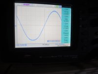
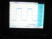
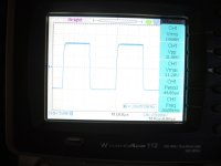
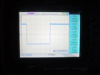
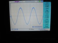
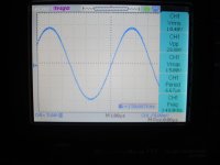
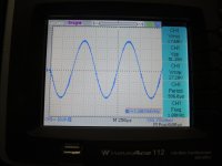
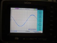
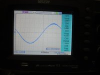
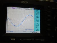
Pics showing Input Stage, Sine Wave measurements @50 % also Square Wave measurements at 75%, then Rail Voltages a little bit higher than it will be when the AMP has it's output Transistors connected.. then Rail Voltage will be 76Volts or 38+ and 38-Volts.
Be back later as soon heat sink has been done..
Regards Chris
First off, just for everybody to understand this is a PROTOTYPE BOARD, to test the Amplifier before it is going to be build, with the real PCB..
And because of that some test haven't passed in the past days it looks how it looks..
There are some important changes since last night:
Test which are listed in Post 22 have all passed up to test Number 6.
Tests have also passed frequency response up to 250KHz. Distortion less than 0.01%
Also tested which is not listed above, is the SERVO CONTROL to make sure that output will be 0.00000Volts all time when amp is running within limits. I know it will be something about 0.05 millivolts up to 5millivolts.. but I can live good with that, because this is something very hard to be detected by human ears.
Now there is some mechanical Work to be done. I do not use conventional Heat sinks for the drive Transistors, so this will DIY heat sinks to have the Drive Transistors all on the same Temp this means one Heat sink for these three Transistors, this is what has to be constructed today.
Pics showing Input Stage, Sine Wave measurements @50 % also Square Wave measurements at 75%, then Rail Voltages a little bit higher than it will be when the AMP has it's output Transistors connected.. then Rail Voltage will be 76Volts or 38+ and 38-Volts.
Be back later as soon heat sink has been done..
Regards Chris
Attachments
-
 1. Khz Sine 10Volts RMS.jpg107.2 KB · Views: 126
 -
 9. Measuring Rail Voltage Amplifier.jpg241.1 KB · Views: 52
 -
 8. Rail Voltage Amplifier.jpg171.2 KB · Views: 64
 -
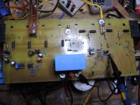 7. Board Top View.jpg286.1 KB · Views: 57
 -
 6. 50Khz Square 10 Volts.jpg188.4 KB · Views: 46
 -
 5. 20khz 10 Votls Square = 14.4 volts Sine.jpg150.3 KB · Views: 102
 -
 4. 1Khz Square 10Volts = 14.4 Volts Sine RMS.jpg114.1 KB · Views: 101
 -
 3. 250Khz Sine - 1db.jpg175.4 KB · Views: 109
 -
 2. 150khz Sine 10.4Votls RMS.jpg138.7 KB · Views: 114
Last edited:
It's coming better everyday
Hi guys
So, the Varaible Current Source Class A AMP is on.
Had a few hickups, but this is a normal thing when doing all DIY.
This is PROTOTYPE..
Here a few pics from today when I had some spare time to work on it..
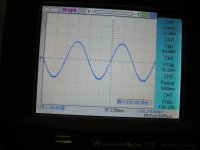
Present time Max Output into 8 Ohms @ 1khz 20.8 Volts RMS this equals 54. Watts RMS, this also counts for all frequencies above 1KHZ up to 150KHz.
Lower frequenceys the Amp is boosting the signal by 0.8 Volts to 21.6 which would be 58.8 Watts RMS.
This is just a small thing to correct, as the input Cap is rather large with 50uf..
When the final PCB and final Circuit is made, which I'm still testing, then the AMP will be linear like 0.0 db 10 - 100Khz..
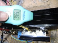
this all with a current flow of 2.33 Ampere, and idle is only 580ma.. this by +- 42 volts Railvoltage is 42 * .58 = 24.36 Watts IDLE Heat. not at lot for a CLASS A
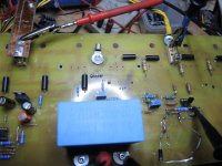
Pics also showing some temps of the Drive unit and the output unit which is not fully installed only 4 output Transistors are used to test. Because all these components will be left on that Prototype.
Next PCB = New Components..
In the mean time I made some changes to the circuit, which unfortunately makes the amp lose some output power but it will be even more Stable. As soon I have tested that in real time I will show a copy here..
But just one thing ahead of time: Dual Current Source feeding, this to even can cut down power more when @ IDLE.. BUT STILL FULL CLASS A.!
Thanks for reading.
Regards Chris Hess
Hi guys
So, the Varaible Current Source Class A AMP is on.
Had a few hickups, but this is a normal thing when doing all DIY.
This is PROTOTYPE..
Here a few pics from today when I had some spare time to work on it..
Present time Max Output into 8 Ohms @ 1khz 20.8 Volts RMS this equals 54. Watts RMS, this also counts for all frequencies above 1KHZ up to 150KHz.
Lower frequenceys the Amp is boosting the signal by 0.8 Volts to 21.6 which would be 58.8 Watts RMS.
This is just a small thing to correct, as the input Cap is rather large with 50uf..
When the final PCB and final Circuit is made, which I'm still testing, then the AMP will be linear like 0.0 db 10 - 100Khz..
this all with a current flow of 2.33 Ampere, and idle is only 580ma.. this by +- 42 volts Railvoltage is 42 * .58 = 24.36 Watts IDLE Heat. not at lot for a CLASS A
Pics also showing some temps of the Drive unit and the output unit which is not fully installed only 4 output Transistors are used to test. Because all these components will be left on that Prototype.
Next PCB = New Components..
In the mean time I made some changes to the circuit, which unfortunately makes the amp lose some output power but it will be even more Stable. As soon I have tested that in real time I will show a copy here..
But just one thing ahead of time: Dual Current Source feeding, this to even can cut down power more when @ IDLE.. BUT STILL FULL CLASS A.!
Thanks for reading.
Regards Chris Hess
Attachments
-
 7. 1Khz Sine - 20.80 Volts RMS into 8Ohm.jpg163.4 KB · Views: 46
 -
 6. 100Hz Sine - 21.6 Volts RMS into 8 Ohms.jpg171.8 KB · Views: 60
 -
 5. Temp Heat Sink Output Stage.jpg171.8 KB · Views: 51
 -
 4.Temp Drive Stage Class A.jpg199.8 KB · Views: 51
 -
 3. Medium Current Selected for bias Class A.jpg190 KB · Views: 62
 -
 2. Variable Current Source Class A - Under Test.jpg208.7 KB · Views: 68
 -
 1. Variable Current Source Class A - Under Test.jpg206.8 KB · Views: 76
Low Frequency specs
Good Morning everybody
So this morning @7am I sat on my construction table and made some adjustments to that Class A amp.
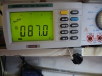
But first pics shows IDLE CURRENT without signal and second Pic shows Current Flow at 38 Watt @1Khz.
Then also:
I needed to get that Low Frequency boost to a lower spec.
Here are the outcome of that,
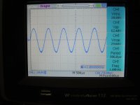
Pics are showing Sine Wave 10 (9.74) Hz to 214Khz @approximately 1 WATT RMS..
Steps are 10hz, 20hz , 2k and 214 KHz.
There are other tests to follow as well other adjustments to be made..
Just besides that, Sound is fantastic..
Guys have a nice day
Good Morning everybody
So this morning @7am I sat on my construction table and made some adjustments to that Class A amp.
But first pics shows IDLE CURRENT without signal and second Pic shows Current Flow at 38 Watt @1Khz.
Then also:
I needed to get that Low Frequency boost to a lower spec.
Here are the outcome of that,
Pics are showing Sine Wave 10 (9.74) Hz to 214Khz @approximately 1 WATT RMS..
Steps are 10hz, 20hz , 2k and 214 KHz.
There are other tests to follow as well other adjustments to be made..
Just besides that, Sound is fantastic..
Guys have a nice day
Attachments
Hi Guys
After extensive testing of the Amp following improvement need to be made.
1.Design a new Double Sided PCB
Same Length but may a bit smaller right now it's 300mm*140mm
New one might be only 300mm*120mm which will make it necessary to drill new TABS into the Aluminum Heat Sink for the stand offs which are fixing the board to heat sink.
2. All transistor will be installed directly to the large Heat Sink
with this I mean Output Transistors, Drive Transistor and also Impedance Change Transistor *Q2* The reason for this is that Drive Transistors getting far too hot, even with cut down BIAS and the Heat Sink these are mounted on is quite large for 3 TO220 Transistor, Temp still rises to 88.5 Degrees Celsius. so moving them to the large heat sink will hopefully correct this problem
3.Only input Transistor, Servo Control, Regulators will reside on top of the PCB.
4. Tracks will be kept as short as possible..
And you can believe me, this Class a runs on full Load @60 Watts 22Volts RMS into 8Ohms with 2.8 Amps - measured with real Speakers connected and on 4 Ohms with 4.3 Amps @ 77Watts = 17.6 Volts RMS, more connecting 2 Ohms or less, don't stresses the AMP
5. Circuit modifications: ZD1 will be removed, because it's reducing performance and making it hard to set 0.000Volts DC at the output.
6. Bias Resistors for Q7 Q8 =2.2Ohm will be exchanged with a Constant Current Source Transistor thus making it possible to run that CLASS A almost COLD, when on IDLE.!
That's all for today
Regards
Chris Hess
Last edited:
Guys
Here some realtime tests of this amplifier.
And don't forget the Amp isn't finish yet, there is some more work to be done
But the main goal has been reached already CLASS A on LOW CURRENT while IDLE.!
The early Clip on the HIGH Frequencies are because I still run the amp not on full Current because other wise BIAS Transistor will blow, and at Present time there is no need to go all the way I will be back with the full capability of this AMP, as soon the NEW PCB are made,.. takes a week or so.
May you take your time to watch the video..
Thanks
Testing Class A Variable Current Source Amp - YouTube
Last edited:
5 Goals set for this amp prior to starting with it.
The 5 Goals I try to achieve making this CLASS A AMP are following:
1. Class A Single End Amp
2. Low Idle Current Consumption max 35Watts if possible only 20 Watts heat while IDLE. it must be Variable Current Source.
3. At least 50 Watts RMS @ 8 Ohms, 70 Watts RMS @ 4Ohms and 100 Watts RMS @ 2 Ohms. Damping Factor better than 150.
4. Maximum 0.01% Distortion @ 1 Watt and 0.2% @ Full load for all loads, as well as for the full Bandwidth of 10hz - 100Khz
5. Low Heat, while the Amp is in IDLE Status, No Ventilation Fans. This means Passive Cooling only.
I actually have a 6th point in mind, but this is rather hard to achieve, as least components as there it is possible.. but this is almost and I think will stay a "dream" !
Sadly, these Goals haven't been reached at all. I've got Goal number 1, number 3, number 4 already the other 2 Goals I'm still working on.
Goal number 2 is has not been possible yet, because amp still is unstable at times, but changing when increasing Idle current for the Variable Part of it.
Goal number 5 has also not be reached till now, because drive Stage gets up to almost 100 degrees Celsius, even with compensated bias current.
So hang in there, I will be back soon. Just got notice, that the ordered double sided PCB have been shipped. should arrive Tuesday or Wednesday from Germany..
BTW the Pre AMP housing which I ordered for my Class A Pre amplifier and line drive has arrived today..
Have a nice weekend everybody..
Regards Chris Hess
Last edited:
Bad Day or bad luck.
Last week I ordered New Photo PCB's double sided, but these didn't made it to my home.
Package has been received on Tuesday but it was just as empty as a package could be when the goods weren't inside..
This forces me to Postpone the next Test PCB, for another week as newly send hasn't arrived yet..
So, I will be back as soon PCB's have been received.
Guys enjoy weekend..
Saturday, August 28th, 2021 9:18,
Just finished testing Version Number 4 of the SEPP or VCSCLA Amp
Got most problem solved as the biggest one was very questionable Linearty, which before never occured to be problem. With this I mean I had a -3db drop over 20Khz now it seems to be withint specs of about 0.2db or better.
Exchanged Drive Transistors for the ones my Spice Program actually calculated that Amp, and this time it's working like charm. It did not earlier with Version 1and 2 work with these Transistors, those would shorten out while Startup.. meaning switch on the AMP or just by pushing the power Switch.
So Version 3 I Tested other Drive Transistors but these unfortunatley couldn't made high frequencies in the range of 100Khz and up. So, tomorrow is the day to get a read out with REW simultanousely with the Osciloscope and Distortion analizer..
One thing is alredy sure: Output voltage at 2Ohm 16 Volts RMS.. 22Volts @ 8 Ohms..with an Idle current of 350ma...
BTW, Temp was around 40 degress after a two hour Stress test.. and the most important thing is: No Fans used.
My Wall outlet Wattmeter presents me a Watt Usage of 35 Watts while Idle..
And we are talking here about a CLASS A with Rail voltage +- 41.5 Volts when Idle and +-38.5 when on Full Load 2 Ohms..
Pics are following tomorrow..
Gents have a nice day, night or what ever it might be..
Greetings
Chris Hess
Last edited:
So as I stated I made another new PCB, because I have seen after drilling it. So this is PCB Number 3 then..
It might be that another one must or will follow, cause if there is anything which turns out for the better, then I will imply that.. and as long this is only a empty PCB with almost no value *Money* so it don't hurt to do it over again.
here I have posted it on my other thread about creating a PCB...
A nice Sunday everyone,
Chris
So as you could read in my other thread BOARD number 5 has been finished and resized.
But instead of assembling the new board I was trying again to get the last bugs out of board number 2. Even sound was fantastic and everything was almost working as *My Computer Calculated for me* there was still a big BUG in it..
High frequency's above 10KHZ was dropping to -3db @100Khz.. I talked to a wise man, and he himself told me.. * That's good enough, hold it right there otherwise you might get unwanted Problems* He sure was exactly right,, Because my EGO wouldn't listen to his advice, and even Now I got what I want meaning 10Hz - 100Khz +- 0.1db @ full load and distortion less than 0.1% I had to reduce the Rail Voltage by 7 Volt. down to 35Volts.
The problem of this -3db drop above 10Khz was only the Transistors which would not meet specs. Even I changed them and I'm sure I got real ones and no fakes, for the drive and Current Source Drive, was not possible to achieve without blowing exactly this stage 10times when using the Transistor I actually wanted to use, which are BD139-16
They would not survive the Switch power on Status. So I exchanged them with several High Power Transistors, but all of them made that -3db Drop..
These were C5200, MJE15032, MJE15034 BD243G the latter one would also blow up on fast Signal changes. The Rest of it would leave with this -3db and crossover Distortion there because of not enough current. Increasing the current would also Change IDLE Current which I set at 300ma..
I know I could use a Thermistor or likewise, but, I do not like these things that much.
As I want to make a Variable Current Source Class A Single End Amp, I need to keep the Idle as low as possible.. So I sacrifice the Output Power @ 8Ohm by about 10 or more Watts.. Nobody is listening full load all the time anyway, and First Watt Comes First and these First Second and Third Watt are the ones I'm interested in.
Tomorrow, I will make a Video of the Test then you guys who saw the last Video on U-Tube can see the difference. Now My goal is to build that LOW CURRENT CLASS A..
The sound is wide and very Clear..
But it was a hard piece of work. And I hope tomorrow it will still work as just an hour ago when I left my working table.. LOL
Guys enjoy Sunday and Weekend as I will do as well..
Greetings,
Chris Hess
Good Morning or Day
on that beautiful Sunday morning October 3rd 2021..
I felt that, and when I went into my working room, I managed to blow up that Prototype already twice again. It runs just fantastic, just to blow up on fast Frequency changes, when testing on the Scope, not while it's Running in regular mode, meaning hearing music..
I think I get reverse Voltages on the Drive Transistor which exceeds that 100 Volts Vceo so that it destroys that Transistor, even at present Time the Amp is running on 72Volts rail only,+36 -36.. and only a mere of 0.3ampere Idle.. Will add a schematic later today of this section..
It could also be that I got a bad Batch of Transistors, which do not meet the specs..
Later
chris
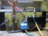
Another step in creating a Variable Current Source Class A Amplifier
Friday morning October 8th 2021 07:47, listening again to that prototype which almost get me out of my mind. We could call it Failure Amplifier.. LOL
Now, after exchanging Transformers from 30 - 0 - 30 AC to 25 - 0 - 25 AC and also exchanging Current Source Transistor the Amp runs stable as pure CLASS A. My Goal is it to run that Amp on 42Volts Rails. not 35
This are facts today, these might change in the next future days--
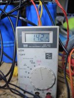
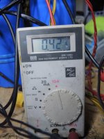
Measured Values
Vrail +- 34 Volts
Idle 0.35Ampere
Power consumption for one Channel 31.3Watts.
Bandwidth 10Hz - 100Khz @ = -1dbDistortion = 0.1%
@ 60Watts 2 Ohm Loudspeakers NOT DUMMY LOAD RMS
Drawing 2.5 Ampere Current from PSU. Measured RMS
Bandwidth 10Hz - 100Khz = - 1db @ Distortion = 0.01%
@ 1Watt 2 Ohms Loudspeakers NOT DUMMY LOAD RMS
Have not measured 4 and 8 Ohms yet.
This will be measured in the next step
Sound is good
Future tasks to check are, Servo Control does not work as Expected when Load is changing at the output of the Amplifier, between 2 Ohms and Dummy load and 2 ohms Loudspeakers
And I need to create a new PCB one more time, this then will be Number 6.
Be back later with pictures
Gents, enjoy the day and life..
Regards Chris Hess
Friday morning October 8th 2021 07:47, listening again to that prototype which almost get me out of my mind. We could call it Failure Amplifier.. LOL
Now, after exchanging Transformers from 30 - 0 - 30 AC to 25 - 0 - 25 AC and also exchanging Current Source Transistor the Amp runs stable as pure CLASS A. My Goal is it to run that Amp on 42Volts Rails. not 35
This are facts today, these might change in the next future days--
Measured Values
Vrail +- 34 Volts
Idle 0.35Ampere
Power consumption for one Channel 31.3Watts.
Bandwidth 10Hz - 100Khz @ = -1dbDistortion = 0.1%
@ 60Watts 2 Ohm Loudspeakers NOT DUMMY LOAD RMS
Drawing 2.5 Ampere Current from PSU. Measured RMS
Bandwidth 10Hz - 100Khz = - 1db @ Distortion = 0.01%
@ 1Watt 2 Ohms Loudspeakers NOT DUMMY LOAD RMS
Have not measured 4 and 8 Ohms yet.
This will be measured in the next step
Sound is good
Future tasks to check are, Servo Control does not work as Expected when Load is changing at the output of the Amplifier, between 2 Ohms and Dummy load and 2 ohms Loudspeakers
And I need to create a new PCB one more time, this then will be Number 6.
Be back later with pictures
Gents, enjoy the day and life..
Regards Chris Hess
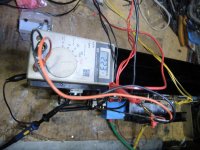
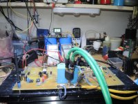
Completing the Boards
Hi Gents
In the meantime I found the bug, which gave a headache for quite some time.
Last Saturday I made two new boards and right now populating them with everything to get that Amp finished (the boards) by end of month..
It looks good that this happens.
Since heatsinks are somewhat smaller than the ones I usually use, I now must design a Chassis or Box or enclosure.. so this will take some time after design to produce..
So, in a few days I will release the Test and also the final circuit of this Variable Current Source Class A Amplifier. A Class A which does not get hot while on Idle.. Also not getting hot while running in rook level listening mode.
I have to say that Distortion is slightly higher than with a Constant Current Source Class A - but this in not in the hearable range . Far below 0.5%. As idle current is as low as 0.30 Amps instead of 4 Ampere as for the hot Single End Class A.
Regards
Chris Hess
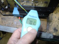
Variable Current Source Class A LOW IDLE NO HEAT
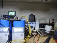
Good Morning Gents
Friday 8:25 22nd October 2021
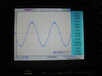
A few pics from that Amp Variable Current Source Class A - output 1 Watt into 2 Ohms
Line Power consumption in the back
Vrail
And Current
Good Morning Gents
Friday 8:25 22nd October 2021
A few pics from that Amp Variable Current Source Class A - output 1 Watt into 2 Ohms
Line Power consumption in the back
Vrail
And Current
Attachments
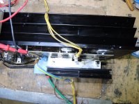
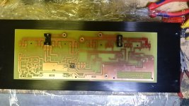
Ready to manufacture
Getting the boards ready to place on Heat-sinks.
Already Through Hole connected and by tomorrow one Side will be assembled for testing, if it passes then second Side will be assembled.
Check the pic
Enjoy Weekend
Getting the boards ready to place on Heat-sinks.
Already Through Hole connected and by tomorrow one Side will be assembled for testing, if it passes then second Side will be assembled.
Check the pic
Enjoy Weekend
Attachments
- Home
- Design & Build
- Construction Tips
- Which Class of Amplifier would this Schematic fit in?