Guys
it's ridicoulous that after 40 years of manufacturing PCB's I don't get the point what is going wrong with my manufacturing PCB..
I use Bunggard 35um PCB. Fotopositive.
Later days I use Tracing paper as Film as well as Laser Film. Both were working good. but lately problems occured I never thought of it..
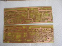
I get bad results when etching the PCB with Ferro Chlorid 3.
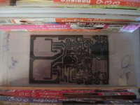
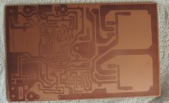
Instead of edging the exposed sequences of the PCB it eats up the Laqeur of the portion which should be the tracks,,
I ordered about 20 Plates PCB with size of 10cm * 16cm. The half of it I had to throw away because at edging all of them were useless..
I use the same Printer, The same Glasses, the same Ultraviolet lamps, exactly the correct exposure timing. and and and and
I always use new devloper, same Edging solution measured by weight. mixed by weight to a 10th of a gramm exact.
And still got to many failures..
and it doesn't matter if I use Film or Tracing Paper.. Finally I think that I got old PCB material from that Store I buy these.
I always measure developer Temp very exaclty 20degrees Celsious.
14 Days ago I again got failing PCB,s so I changend the Edging ACID to Natriumpersulfat. I almost died because the Air vent Failed and to this day I'm feeling sick, lost my short time memory to a big degree, sometims walking around like drunk. and if I sit down or lay down everything is turning like o a carusel. And I do not drink or smoke nor smoinkg pot.. nor taking drugs.. just 5 minutes of this poisoned air of this NATRIUMPERSULFAT almost make me to a usless Person.
And I can't take off from work, because there is nobody to do my work.. But this aint a problem.. but the bad PCB's is a big problem I can not finish my testing with such boards.
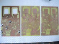
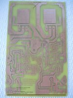
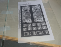
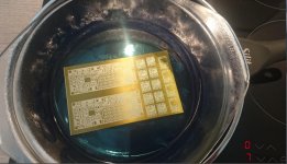
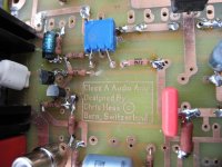
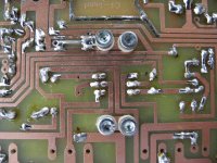
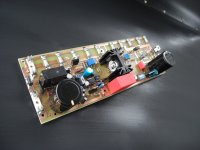
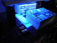
Show you a good one and the ones with very strange structure..
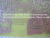
What makes it more strange, it kill the BIG TRACKS not the small ones.. LOL
Check out the pics please..
May some of you have seen something like that before..
Let me know if you think you know the reason..
Thanks MANY Thanks..
Regards Chris Hess
it's ridicoulous that after 40 years of manufacturing PCB's I don't get the point what is going wrong with my manufacturing PCB..
I use Bunggard 35um PCB. Fotopositive.
Later days I use Tracing paper as Film as well as Laser Film. Both were working good. but lately problems occured I never thought of it..
I get bad results when etching the PCB with Ferro Chlorid 3.
Instead of edging the exposed sequences of the PCB it eats up the Laqeur of the portion which should be the tracks,,
I ordered about 20 Plates PCB with size of 10cm * 16cm. The half of it I had to throw away because at edging all of them were useless..
I use the same Printer, The same Glasses, the same Ultraviolet lamps, exactly the correct exposure timing. and and and and
I always use new devloper, same Edging solution measured by weight. mixed by weight to a 10th of a gramm exact.
And still got to many failures..
and it doesn't matter if I use Film or Tracing Paper.. Finally I think that I got old PCB material from that Store I buy these.
I always measure developer Temp very exaclty 20degrees Celsious.
14 Days ago I again got failing PCB,s so I changend the Edging ACID to Natriumpersulfat. I almost died because the Air vent Failed and to this day I'm feeling sick, lost my short time memory to a big degree, sometims walking around like drunk. and if I sit down or lay down everything is turning like o a carusel. And I do not drink or smoke nor smoinkg pot.. nor taking drugs.. just 5 minutes of this poisoned air of this NATRIUMPERSULFAT almost make me to a usless Person.
And I can't take off from work, because there is nobody to do my work.. But this aint a problem.. but the bad PCB's is a big problem I can not finish my testing with such boards.
Show you a good one and the ones with very strange structure..
What makes it more strange, it kill the BIG TRACKS not the small ones.. LOL
Check out the pics please..
May some of you have seen something like that before..
Let me know if you think you know the reason..
Thanks MANY Thanks..
Regards Chris Hess
Attachments
-
 1. PCBs.jpg188.9 KB · Views: 214
 -
 7. Small letters OK thick line bad.jpg162.1 KB · Views: 65
 -
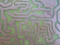 6. lines ugly.jpg178.3 KB · Views: 79
 -
 5. Bad Edging - Swollen up lines..jpg218.7 KB · Views: 204
 -
 4.Bad PCB yesterday.jpg340.6 KB · Views: 160
 -
 3.Good small letters OK - Thick lines OK.jpg151.7 KB · Views: 220
 -
 2. good pcb.jpg158.6 KB · Views: 217
I see various problems.
In no particular order:
1) you have *contact* problems.
The artwork sheet is not firmly pressed against the photoemulsion and light enters through the borders into areas which "should" be covered, this is specially noticeable at the edges because it´s always hard to keep uniform pressure there.
On top and bottom edges and partly onnthe left one, you not only lost fine tracks and text but even chunks of large flat areas.
2) your toner is not black enough.
The very same laser printer which worked fine months ago either is near the end of its toner cartridge (which can be solved by getting a new original one, no refills or recycled ones for PCB artwork, sorry) or the photosensitive image drum inside the printer is getting old.
I recently replaced my faithful workhorse Lexmark Optra + which had been used *exclusively* for PCB and silkscreen (front panels and PCBs) for over 10 years (It was still in "as new" condition) because of that.
I bought a new cheap Samsung printer, it prints carbon black thick toner, I suggest you get one too.
3) even so, toner being a "dust" type "ink" by definition can and will have micropores and pinholes here and there, your old printer simply has thousands of them all over the place, because although black plastic (toner) particles partly melt so as to stick to paper, they never become a real liquid, so one molten grain may not fully join its neighbour, leaving a micro hole in between.
4) there is a "toner blackener" spray can, ask about it at Graphics supply shops, Printers have the same problem as us and use it to improve quality, it contains a little solvent which partially melts toner, en result is blacker because it covers better.
Don´t use too much because it can make a mess.
5) IF you use Vellum (tracing paper) put toner side in direct contact with photoemulsion, I do that when burning silkscreens.
PRO exposure machines use vacuum to ensure perfect contact.
If you just use a piece of glass and its own weight, good contact is NOT assured.
6) or forget Vellum , print 2 crystal clear transparencies on polyester film, align and tape them,you will be surprised at blackness achieved, and use them instead.
7) if you are using a bed of many UV tubes, that´s diffused light, easy to go where you don´t want it, try to use single UV lamp (point source) some 60cm above the exposed board, you will have much cleaned edges.
8) just in case, show a picture of your exposure setup.
9) you *might* have a batch of older PCB material , try etching *unexposed* - half exposed and fully exposed material so as to put artwork out of the way.
Even better, use guaranteed opaque material (such as a coin) on the partly and fully exposed bits and see what happens.
Last edited:
Natrium- or Ammoniumpersulfat does not generate poisonous air. It is
just acid with some excess O2. The solution must not cook. When you
see the first bubbles, it's time to turn off the heating immediately.
I print the circuit on "Avery-Zweckform-Folie zu Erstellung von Photoformat-
Vorlagen" on a Kyocera color laser printer. The OKI I had before was better.
The foil is somewhat milky with a non glaring surface. That's no drawback
because the toner is in direct contact to the photo layer.
If it really counts, like for microwave filters, I go to the next print shop
and have them make me an offset film on their Agfatronik or Linotype with
true 2400 dpi. Then black is absolutely black, and translucent really translucent.
It usually costs 5-10€ into their coffee box for DIN/ISO A4 oversize.
They accept normal .pdf 1:1. You can make a check plot on your printer.
I must print it 4% larger on the Kyocera, so an Euro card is really 100*160mm.
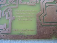
Board material is Bungard, I buy it at Segor.de because I know them from
my time in Berlin.
just acid with some excess O2. The solution must not cook. When you
see the first bubbles, it's time to turn off the heating immediately.
I print the circuit on "Avery-Zweckform-Folie zu Erstellung von Photoformat-
Vorlagen" on a Kyocera color laser printer. The OKI I had before was better.
The foil is somewhat milky with a non glaring surface. That's no drawback
because the toner is in direct contact to the photo layer.
If it really counts, like for microwave filters, I go to the next print shop
and have them make me an offset film on their Agfatronik or Linotype with
true 2400 dpi. Then black is absolutely black, and translucent really translucent.
It usually costs 5-10€ into their coffee box for DIN/ISO A4 oversize.
They accept normal .pdf 1:1. You can make a check plot on your printer.
I must print it 4% larger on the Kyocera, so an Euro card is really 100*160mm.
Board material is Bungard, I buy it at Segor.de because I know them from
my time in Berlin.
Attachments
Last edited:
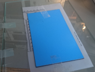
The film and the board are mounted between 2 thick glass plates.
One side is normally reserved for ground an not etched at all.
No alignment problems and good ground is important.
Yes, the universe is held together by duct tape.
One side is normally reserved for ground an not etched at all.
No alignment problems and good ground is important.
Yes, the universe is held together by duct tape.
Attachments
Last edited:
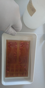
Etching is in persulfate, I now have an induction stove which
complicates things. I use an enameled Silit pan with some
water in it to get some energy from the field and a Pyrex
glass pot in it that contains the persulfate solution.
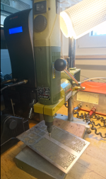
Drilling is on a Proxxon drill with hard metal bits at elevated RPM.
Please do wear goggles. Having the tip of a wolfram drill bit
in the eye is probably no fun.
complicates things. I use an enameled Silit pan with some
water in it to get some energy from the field and a Pyrex
glass pot in it that contains the persulfate solution.
Drilling is on a Proxxon drill with hard metal bits at elevated RPM.
Please do wear goggles. Having the tip of a wolfram drill bit
in the eye is probably no fun.
Attachments
Last edited:
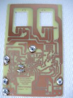
Here Exposure and more
Thanks
1. Floor of the under Glass is a even Granit Stone Table 100% even and not bend.
PCB to get image is glued against it on a 5mm thick Glas Plate. Size A3
Cover Glas plate is 1mm thick and Pressure is 5KG per side. on the long sides.. Artwork lays with the Printed side agains the PCB--
2.Yes for The Toner.. It might be that one.. Its a OKI Printer, and the Printer screams to have the drum replaced-- It's ordered-.. will arrive next week.
3 & 4. OK but I did not use till today
5. I always put that Printed side onto the BOARD SIDE
6. have tried that before edges are not sharp, BTW it's a painstaking Work to align this so that every small piece is set straigt to the other.. and forget about if you make doublesided PCB.. Have Tried it-- Usually I make good boards.
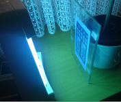
7. I use 2 x18 Watts Philips Ultraviolet lamps laying besides each other in a Frame. Before I use them to expose the boards I let them warm for 10 minutes..
Distance to the Artwork is 15cm, I checked with a light scale that all the suare has the same lumination .. this is given +- 0.5% on the size of A3 Space. This boards are only not even A5.
8. Exposure setup is
a, Granit Table
b. 5mm thick clean and dust, oil and grease fress glass plate A3
c. PCB glued with thin duct tape against it on the back side.
d. Artwork covers the PCB and is fixed one side and then STRECHED to get waves out, and then fixed with duct tape again.
e. Top glass 1mm thick each side has a wheight of about 1.5 kg. this if all 4 sides are pressed equals 6 Kilos pressure on that Glas.
f. on the long side there is two Aluminum BLACK 16CM high HEATSINK which is the holder where the LAMP locks in on top of that. straight over the PCB
g. Exposure time for single side PCB with LASER FILM 90 Seconds with Transfer paper 180 seconds. this I test each time before I use the real one.
9. Good Idea, will do that.
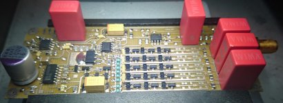
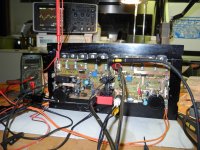
I show you how I made PCB 2013 and all of them came out just beautiful could win a contest. check out the pics and Laugh.
And Many Thanks.. because you give me the solution already with number 2.
Regards
Chris
Thanks
1. Floor of the under Glass is a even Granit Stone Table 100% even and not bend.
PCB to get image is glued against it on a 5mm thick Glas Plate. Size A3
Cover Glas plate is 1mm thick and Pressure is 5KG per side. on the long sides.. Artwork lays with the Printed side agains the PCB--
2.Yes for The Toner.. It might be that one.. Its a OKI Printer, and the Printer screams to have the drum replaced-- It's ordered-.. will arrive next week.
3 & 4. OK but I did not use till today
5. I always put that Printed side onto the BOARD SIDE
6. have tried that before edges are not sharp, BTW it's a painstaking Work to align this so that every small piece is set straigt to the other.. and forget about if you make doublesided PCB.. Have Tried it-- Usually I make good boards.
7. I use 2 x18 Watts Philips Ultraviolet lamps laying besides each other in a Frame. Before I use them to expose the boards I let them warm for 10 minutes..
Distance to the Artwork is 15cm, I checked with a light scale that all the suare has the same lumination .. this is given +- 0.5% on the size of A3 Space. This boards are only not even A5.
8. Exposure setup is
a, Granit Table
b. 5mm thick clean and dust, oil and grease fress glass plate A3
c. PCB glued with thin duct tape against it on the back side.
d. Artwork covers the PCB and is fixed one side and then STRECHED to get waves out, and then fixed with duct tape again.
e. Top glass 1mm thick each side has a wheight of about 1.5 kg. this if all 4 sides are pressed equals 6 Kilos pressure on that Glas.
f. on the long side there is two Aluminum BLACK 16CM high HEATSINK which is the holder where the LAMP locks in on top of that. straight over the PCB
g. Exposure time for single side PCB with LASER FILM 90 Seconds with Transfer paper 180 seconds. this I test each time before I use the real one.
9. Good Idea, will do that.
I show you how I made PCB 2013 and all of them came out just beautiful could win a contest. check out the pics and Laugh.
And Many Thanks.. because you give me the solution already with number 2.
Regards
Chris
Attachments
Your word in my ear
Es hat mich fast umgebracht.. It almost killed me..
Nice job you done there..
and yes JMFahey he saw this on the PCB's that toner is bad.. because I did not place the Artwork. here..
Guys thank you so much for your inputs. it's appreciated and I'm feeling better,
@Gerhard. Danke schön.
Gruss aus der Schweiz
Regards Chris
Since I had my head over it last friday 14 days ago.. I can't think clear.. this to none poisonous..Natrium- or Ammoniumpersulfat does not generate poisonous air. It is
just acid with some excess O2. The solution must not cook. When you
see the first bubbles, it's time to turn off the heating immediately.
Board material is Bungard, I buy it at Segor.de because I know them from
my time in Berlin.
Es hat mich fast umgebracht.. It almost killed me..
Nice job you done there..
and yes JMFahey he saw this on the PCB's that toner is bad.. because I did not place the Artwork. here..
Guys thank you so much for your inputs. it's appreciated and I'm feeling better,
@Gerhard. Danke schön.
Gruss aus der Schweiz
Regards Chris
Same here
I use Carbon drills these brake faster than Wolfram but don't fly around..
Buy them in Friedrichshafen @ Ham Radio Messe. I'm there almost every year.
But this year not as Corona took over the world..
Build a small machine just to shake the pcb while edging,. using Ferro Chloride 3, usually gives good results.
What is the mixture you use with Natrium? 1dl Water 30 Grams Natrium?
Drilling is on a Proxxon drill with hard metal bits at elevated RPM.
Please do wear goggles. Having the tip of a wolfram drill bit
in the eye is probably no fun.
I use Carbon drills these brake faster than Wolfram but don't fly around..
Buy them in Friedrichshafen @ Ham Radio Messe. I'm there almost every year.
But this year not as Corona took over the world..
Build a small machine just to shake the pcb while edging,. using Ferro Chloride 3, usually gives good results.
What is the mixture you use with Natrium? 1dl Water 30 Grams Natrium?
I use a Nalgene bottle that holds 1l and add 1 good teaspoon of NaOH pellets.
It's really a plastic spoon I got for exactly this. Illuminate a throw-away board until
it has seen enough light for sure and then test the developer solution. It should
not take more than 20 seconds to dissolve most of the resist. Try until you find
a mixture that works to your taste. If it is too strong, it dissolves everything, if
the solution is too weak, there may remain a film that cannot be seen, but it
still inhibits etching.
When you know that your developing solution is OK, you can check the exposure
time. Select one that removes the mask for everything that has been exposed
and lets the rest alone, without holes. Note the conditions, so you can repeat
them . An hour invested here spares you a lot of trouble.
Friedrichshafen was quite a fun last year.
73, Gerhard, DK4XP
Last edited:
This is not Audio or Electronics but relevant to your symptoms: please visit a Doctor, tell him about yoursymptoms and get a thorough check. Not kidding.Since I had my head over it last friday 14 days ago.. I can't think clear.. this to none poisonous..
Es hat mich fast umgebracht.. It almost killed me..
Doubt Ammonium Persulphate was directly responsible but your symptoms are both prolongued and serious.
You were probably anxious or worried about your PCB or something else, and might have had a blood pressure peak or some mini-stroke or other medical condition, or ammonium persulphate was impure and when heated leftb out some evil fumes or ... or ... or ...
Not diagnosing or anything of that kind, by any means, just suggest a Doctor checks you.
PCB etching or not, that´s a relatively minor matter and completely unrelated, just a chance coincidence, but the symptoms alone are worrying, better clear the clouds.
Yes, I know, Covid complicates everything, and in this moment Hospitals are to be avoided unless completely necessary, but maybe a Family Doctor is available.
At least phone him
")
Don't know how access to Chinese companies works for you guys, but I found a while back that I can't possibly get boards made any cheaper, faster, or higher quality than going through PCBway.com. A quick layout in KiCad and send gerbers to PCBway, and boards arrive in about a week, drilled, cut, plated through, silkscreened and solder masked. A whole lot different from when I was etching stuff myself.
This is not Audio or Electronics but relevant to your symptoms: please visit a Doctor, tell him about yoursymptoms and get a thorough check. Not kidding.
Doubt Ammonium Persulphate was directly responsible but your symptoms are both prolongued and serious.
You were probably anxious or worried about your PCB or something else, and might have had a blood pressure peak or some mini-stroke or other medical condition, or ammonium persulphate was impure and when heated leftb out some evil fumes or ... or ... or ...
Not diagnosing or anything of that kind, by any means, just suggest a Doctor checks you.
PCB etching or not, that´s a relatively minor matter and completely unrelated, just a chance coincidence, but the symptoms alone are worrying, better clear the clouds.
Yes, I know, Covid complicates everything, and in this moment Hospitals are to be avoided unless completely necessary, but maybe a Family Doctor is available.
At least phone him
I definitely second that. And one should not be an indirect Covid victim.
Thanks for your help.
@Gerhard @JMfahey
Don't worry about. everything OK so far..
I can assure you that I'm in a perfect health..
Those issues were not, because of something else but
because breathing some of these Natriumpersulfat fumes,
and according to the Label on the Plastic Bottle, these are dangerous when breathing them and gave me a hard time for the following 2 days, 2 weeks ago.
In the meantime everything is OK doctor made a check up last week.
100% as this can be when someone is nearly 70..
Thanks for your Help.
So I can use my freetime otherwise than building Amps today.
In one Project I'm waiting for Transformes to arrive the from USA, and in the other I'm waiting to get a new DRUM drum for my printer so I can make PCB's.
Now I'm playing with the thought of sending the Gerberfiles to Malaysia, there is Silver Circuits Company which makes good Quality PCB's..But, the only thing which is against this, it's each time 3 weeks to get them.. I'm waiting for Material I ordered from Thailand 2 months back and it still sticks at Suvarnabhum Airport in Thailand because of what I don't know.
@gerhard, I will be always at HAM RADIO in Friedrichshafen on FRIDAY..from 9 am to 1 pm, this becasue of the long way from Bern to there. Takes me 3 hours by car, if I keep the Road rules and drive in normal manner..
@JMFahey can you tell me the Model Number or Modelname of that Samsung Printer?
I have here 4 Printers but two of them are Inkjets and I already tried them, even are high quality Canon fotoprinters, the results when printing Films or Tracing paper are not overwhelming.. The 3 Printer is also a OKI and this one also needs Black Drum and Color. And the one I acutally use for these things, which is telling me please exchange Black Drum, but it prints for ages since that notification on the display..
Guys Thanks - Next PCB when material has come will be shown here.
Chris
@JMFahey @Gerhard
I gave it another try. Controlled all I could..
Made that Film REAL BLACK Printed it two times with another LASER I HAVE - Talking about Tracing paper. I can make pictures for you.. but I'm fed up for today.. it's the PCB's which are old. not going to order again from that shop.. Gerhard know them for sure KONRAD..
Cleaned the Glas, Measured Temp on Developer as well as the weight. Extendet the Exposure time by 15 Seconds to 215 Seconds. and used on the long side of the BOARD per Side 6 KG Weights. the Artwork really sticked to it.. and? Just to understand that I don't even EDGED IT YET.. The tracks are a MESH I have never seen before but If I edge them then the same thing will happen.. Going to buy fotopositive spray so I dont need to throw away the pcb. and if it goes bad at that time. then I will take the blame..
Bad Quality and now I pull down the protection sheet of a brand new PCB not Exposed yet.. Forget it. Old Material.. So the rest I send them back ..
Believe me, this is not the first time that I making PCB.. but it's the first time that I had so many Failures.
Every second plate is bad..
Thanks for helping..
Regards Chris
Last edited:
I will take this way as well
I am waiting for an offer from Silver Cirquits in Malaysia.. Have some samples from them.. exactly what I expect for a good Board.
BUT then it's no more DIY to full extend and this small three letters have kept me from sending my files to board manufacturers. this is the only reason. But I want to produce good Work and not work when someone sees's it that these peoples are going to throw up..
It robbed me the rest of confidence into the dealers of these Electronics parts..
Have lived in Thailand, and I saw many shrewed thing. Have travelled in China, never happen that I got bad components there, .. but here in Swiss once in time you got Bad components.. I have straight line how I work and if something is working good for me, then I keep it that way. But out of sudden I can't do my work no more as before or say I work for the Trashcan.. NO NEVER. I will sacrifice that Part of DIY, giving the PCB to them who have the right MACHINES to do that kind of work. NO MORE! Even it cost me more time to test my stuff. but this way is not the way to go..
Thanks guys..
Don't know how access to Chinese companies works for you guys, but I found a while back that I can't possibly get boards made any cheaper, faster, or higher quality than going through PCBway.com. A quick layout in KiCad and send gerbers to PCBway, and boards arrive in about a week, drilled, cut, plated through, silkscreened and solder masked. A whole lot different from when I was etching stuff myself.
I am waiting for an offer from Silver Cirquits in Malaysia.. Have some samples from them.. exactly what I expect for a good Board.
BUT then it's no more DIY to full extend and this small three letters have kept me from sending my files to board manufacturers. this is the only reason. But I want to produce good Work and not work when someone sees's it that these peoples are going to throw up..
It robbed me the rest of confidence into the dealers of these Electronics parts..
Have lived in Thailand, and I saw many shrewed thing. Have travelled in China, never happen that I got bad components there, .. but here in Swiss once in time you got Bad components.. I have straight line how I work and if something is working good for me, then I keep it that way. But out of sudden I can't do my work no more as before or say I work for the Trashcan.. NO NEVER. I will sacrifice that Part of DIY, giving the PCB to them who have the right MACHINES to do that kind of work. NO MORE! Even it cost me more time to test my stuff. but this way is not the way to go..
Thanks guys..
Last edited:
- Status
- This old topic is closed. If you want to reopen this topic, contact a moderator using the "Report Post" button.
- Home
- Design & Build
- Construction Tips
- Help! on Bunggard Fotopositive PCB