Hi,
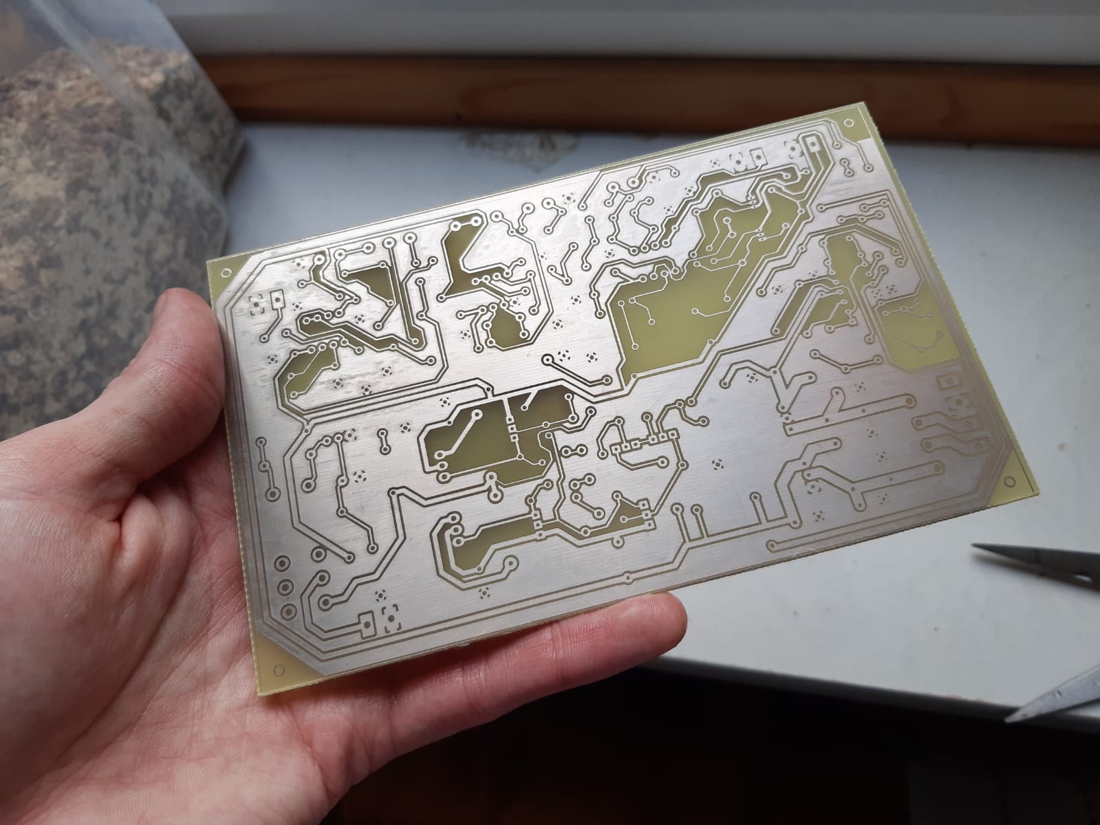
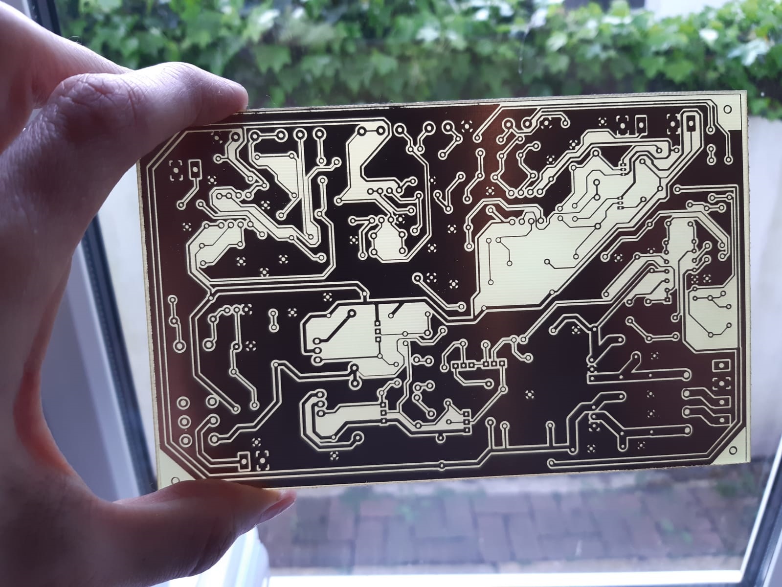
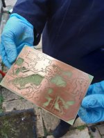
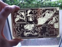
I just wanted to share the results of my first attempt at PCB making.
The board is for a headphone guitar amp and I designed it using EasyEDA. I printed the layout onto tracing paper with a Samsung M2026 laser printer. I made two copies and overlaid them to increase the contrast. I actually had to print several copies to get two that were the same size. It seems that the printer isn't 100% accurate each time.
I used a Bungard pre-sensitised board and exposed it for 6 mins using a MEGA UV exposure unit. I then developed the board in sodium hydroxide for about 30 seconds and then etched in ferric chloride for about 15 minutes. After cleaning off the photo-resist with acetone, I tinned the board in 'seno tin' tinning solution.
I couldn't be happier with how it turned out. I spent a long time reading posts on this forum and in other places to try and avoid making mistakes so I wanted to share my exact method and results in case anyone, like me, is thinking about making PCBs but is worried about how difficult it might be.
I've still got to drill the board, so that's the next challenge, and then see if it actually works! Fingers crossed.

James
I just wanted to share the results of my first attempt at PCB making.
The board is for a headphone guitar amp and I designed it using EasyEDA. I printed the layout onto tracing paper with a Samsung M2026 laser printer. I made two copies and overlaid them to increase the contrast. I actually had to print several copies to get two that were the same size. It seems that the printer isn't 100% accurate each time.
I used a Bungard pre-sensitised board and exposed it for 6 mins using a MEGA UV exposure unit. I then developed the board in sodium hydroxide for about 30 seconds and then etched in ferric chloride for about 15 minutes. After cleaning off the photo-resist with acetone, I tinned the board in 'seno tin' tinning solution.
I couldn't be happier with how it turned out. I spent a long time reading posts on this forum and in other places to try and avoid making mistakes so I wanted to share my exact method and results in case anyone, like me, is thinking about making PCBs but is worried about how difficult it might be.
I've still got to drill the board, so that's the next challenge, and then see if it actually works! Fingers crossed.
James
Attachments

nice, is it important for an audio pcb that the copper surface to be protected?
or is it ok to leave the bare copper film
Very nice board. Usually the copper should be tin or gold plated, to prevent corrosion and
to ease soldering, as he has done.
nice, is it important for an audio pcb that the copper surface to be protected? or is it ok to leave the bare copper film
Copper tarnishes over time, and will then show every fingerprint. You can use clear coat of varnish or conformal coating though.
Copper tarnishes over time, and will then show every fingerprint. You can use clear coat of varnish or conformal coating though.
Don't k now if it's available around the globe -- "Liquid Tin" from MG Chemicals -- contains fluoroboric acid, stannous fluoroborate and thiourea -- will tin coat copper in just a few minutes. You can use it on most substrates, (probably NOT phenolic).
Thanks for all the nice words guys!
I've got a PCB drill coming this week (hopefully) so we'll see how that next stage goes. Is it recommended to lacquer the board after soldering or is tinning sufficient on its own?
I've never tried toner transfer but I got the idea that it was an inferior method. I've seen really nice PCBs made with UV exposure, hence why I decided to go that route.
Thanks,
James
Congratulations!!!
For the next one: tracing paper IS paper, so expands and shrinks depending on humidity, the Laser printer by itself is very accurate.
Use Laser Transparency film instead, which is Polyester.
In my experience, not as dark/opaque as printing on tracing paper (probably depending on surface smoothness) but since it´s exact and crystal transparent two copies are far easier to align for excellent blackness.
I do that to burn my silkscreens, but the occasional photosensitive prototype comes out very well.
Not sure about yours, but on the one I use, I leave the developed Photoemulsion on: looks very nice, protects copper and readily melts/evaporates under solder temperature.
Impressive work for a first attempt! My first PCB's were done by painting etch-resistant directly onto the bare copper Surface, using a quill. Later on I did it the same way like you, but protected the copper traces after etching either by solderable laquer that melts when soldering and acts as a flux as well. Also works with a solution of wood resin in ethylic spirit.
Best regards!
Best regards!
Nice work.
I use this method too.
Just a tip, do not use acetone after etching, just place the board in the exposure unit again, leave it for a long time 10-15 minutes.
Put the board in the sodium hydroxide for a little.
Wash the board with plenty of water.
That's it!
I use this method too.
Just a tip, do not use acetone after etching, just place the board in the exposure unit again, leave it for a long time 10-15 minutes.
Put the board in the sodium hydroxide for a little.
Wash the board with plenty of water.
That's it!
Last edited:
Nicely done, Sir! That is seriously impressive for a first-timer.
If you are concerned about oxidation of the copper, use a conformal coating. Regular clear spray paint works in a pinch. Since regular spray paint is not intended for soldering, it does make rework/repair a bit harder down the road. Some of the conformal coatings are solderable. I'd use one of those.
I've used that as well. It makes for a nice solderable surface (assuming you solder soon after plating). The tin coating does tarnish/oxidize over time.
Mine too. Except with a pen that contained the etch-resistant lacquer. They were known as DALO pens, presumably because DALO made them.
Tom
If you are concerned about oxidation of the copper, use a conformal coating. Regular clear spray paint works in a pinch. Since regular spray paint is not intended for soldering, it does make rework/repair a bit harder down the road. Some of the conformal coatings are solderable. I'd use one of those.
"Liquid Tin" from MG Chemicals
I've used that as well. It makes for a nice solderable surface (assuming you solder soon after plating). The tin coating does tarnish/oxidize over time.
My first PCB's were done by painting etch-resistant directly onto the bare copper Surface, using a quill.
Mine too. Except with a pen that contained the etch-resistant lacquer. They were known as DALO pens, presumably because DALO made them.
Tom
Thumps up for you. Very Impressive. Making PCB for at least 20 years now, now match compared to yours.. your the man.. I thought mine were good.. far off. At a concert they would say .. "Standing Ovation for You"
Congrats
you just give me a Push to make mine better..
Congrats
you just give me a Push to make mine better..
Last edited:
I have to make a New PCB today, later in the afternoon, just single sided..
To drill the holes I use a small Dremel with Carbon drills.. takes a few minutes if you have never done it, but is a lot cheaper than a computerized drill machine.100 holes can be done in 15 minutes and since by the hole for the drill the copper has been removed it's not a big task to center the drill.
Sho w you mine later today as soon its done.
- Status
- This old topic is closed. If you want to reopen this topic, contact a moderator using the "Report Post" button.
- Home
- Design & Build
- Construction Tips
- PCB making - first attempt