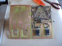
New PCB to next Step of my Project
PCB is done, drilled and spaced for the Transistor.
No to compare to yours, but everything I need is there..
This is version 02 of Class A all Transistor with Servo and Active Cooling-
No Parts will be moved. everything will be build with new components. On the right side the old one.. Working but unstable.
Attachments
I am just about to etch my first pcb , does not look as impressive as yours i have to say ") , i am looking into ways to tin it afterwards , how did you get on with the seno tin ? , i read some poor reviews , the Mg chemical liquid tin seems to be the way to go but its over £80 for a bottle !! ..
, i am looking into ways to tin it afterwards , how did you get on with the seno tin ? , i read some poor reviews , the Mg chemical liquid tin seems to be the way to go but its over £80 for a bottle !! ..
I see they make a smaller bottle but does not seem to be available in the uk , from what i can see..
, i am looking into ways to tin it afterwards , how did you get on with the seno tin ? , i read some poor reviews , the Mg chemical liquid tin seems to be the way to go but its over £80 for a bottle !! .. I see they make a smaller bottle but does not seem to be available in the uk , from what i can see..
Just tin it with your soldering iron.
Just drag a blob of solder around the tracks ?
JamesUK,
An excellent result.
But if you’ll forgive my intrusion, some points that you might consider next time.
While the track integrity is excellent, why make such thin tracks where they’re not necessary. The wider they are, the better the adhesion, so less risk of track lift on repair. I almost always, where possible, make the track the same width as the pad diameter i.e. 0.080”, but then I use liquid photo resist poured onto the bare copper clad, which is more prone to dirt contamination and possible pin holes, therefore track breaks.
Make the annulus at the pads as wide as possible i.e. keep the hole small. I set it at 0.016”. It reduces the risk of damage while soldering, or if repairs are needed, since you’ve much more pad adhered to the board. It also makes for a smaller guide hole for the drill point, thus centring the drill more accurately.
I tend not to flood the board with copper. With my method, ink jet onto transparency, it uses up too much ink, and for audio stuff, isn’t needed. I have far less success using laser.
While transparencies are reasonably stable, I still copy the layout onto the same sheet twice, one alongside the other, depending upon its size, so that any distortion should occur equally. It’s more economical, too.
Brian.
Thanks for the suggestions. As to why the traces are so thin, it's simply because it was my first attempt and I don't fully know what I'm doing yet. I'm working on the design for another board at the moment for another project and I've been making the traces as wide as possible. I also found that some of the default hole sizes are tricky to drill or have too little copper area so I've been fine tuning those on the new board. It's been a good learning experience and I hope etching the next one goes as easily as the first.
- Status
- This old topic is closed. If you want to reopen this topic, contact a moderator using the "Report Post" button.
- Home
- Design & Build
- Construction Tips
- PCB making - first attempt