Mooly, to bad, then someone have bought a great amount of them, 368 do I think.
What are the difference in Carbon and metal film, functionality vise in this circuit?
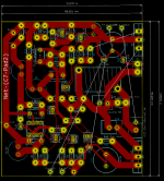
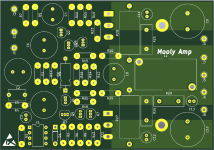
I have added my latest but not finished pcb, but I am thinking of redusing the 4mm traces in most of the board, except in the audio in/out. It will reduce the size of the board, and may not give much more impedance?
What are the difference in Carbon and metal film, functionality vise in this circuit?
I have added my latest but not finished pcb, but I am thinking of redusing the 4mm traces in most of the board, except in the audio in/out. It will reduce the size of the board, and may not give much more impedance?
Attachments
Proper carbon film types can be very good and pretty much everything used them years ago.
Don't confuse true carbon film types with the ancient and horrible Carbon Composition ones.
The 10 ohm resistors in this amp will have no real impact on the sound whatever you use.
Metal film are more stable over time and temperature than carbon film and they have a lower intrinsic noise level, however in a power amp like this the noise factor of the resistors is of no consequence.
The tolerance of normal carbon film type is 5% against 1% or better for metal.
These are typical carbon films:
https://cpc.farnell.com/velleman-sa...f-1-4w-5-e12-610pc/dp/RE07593?st=resistor kit
My take on the various resistor types:
Carbon composition - very distorty, lots of excess noise, drift with age, unstable with humidity and temperature, but can absorb huge power spikes without problem, kW and beyond, which means they still have specialist use in transient absorbtion.
Carbon film - slightly distorty, some excess noise, high tempco, not considered precision.
Metal film (aka thin film in SMT) - almost perfect, various grades of low-tempco available, resistor of choice since 1980's, very high precision versions are available, especially as "metal foil". Small SMT thin-film have the worst performance of this group.
Metal oxide (aka thick film in SMT). Slightly distorty (better than most carbon film), pretty good otherwise.
Wirewound - even more almost perfect(!), but can have unwanted inductance. Used as secondary resistance standards in labs due to stability and linearity.
There are also specialized "fusible resistors" which are designed to always fail open-circuit without starting a fire. Commonly needed in various mains circuits and worth knowing about as they can save you from having a separate protection fuse. Not sure what technology they use, but I suspect its a low-melting point metal film or similar. Standard metal film can glow orange hot on overload, not a safe condition!
May I please ask you if you will upload an image or pdf or your schematic?I had some trouble sleeping yesterday so...
Not really tidied up and optimized but just another example, to show how to better make use of your two layers and maximize copper use.
The mosfet go "under" the pcb, in between the pcb and the heatsink, the leads bent upwards and the whole pcb is attached to the heatsink.
It's so I can better try to find out what component numbers lays were on your schematic.
")
I am trying to train in design of pcb
So if I combine Mooly's and Mark Tillotson's comment, it sounds like a metal film resistor is the best choice?
And don't forget MIL grade too, of course...
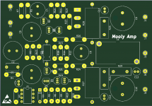
Yes I know it, this is nothing special, and 99% of the design is copied from 00940: Worst PCB track-layout ever?
But I am still satisfied with where my board is heading, I have not yet placed any tracks but hope it will be something I can do in about same style as 00940
EDIT: Forgot to say that the Mosfets are on the backside, but it is not clear from the image.
But I am still satisfied with where my board is heading, I have not yet placed any tracks but hope it will be something I can do in about same style as 00940
EDIT: Forgot to say that the Mosfets are on the backside, but it is not clear from the image.
Attachments
Last edited:
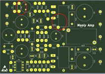
I see no mount holes on your PCB. You also need them for the MOSFETs to tighten them to the heat sink. I would recommend to use standard 0.1" or 0.2" spacing for the input and output pads. You can use a standard connector footprint for this even if you do not plan to use it.
Note: when you show the PCB design without showing traces it is impossible to see the quality of routing.
Regards,
Oleg
Note: when you show the PCB design without showing traces it is impossible to see the quality of routing.
Regards,
Oleg
Ups, did misread your comment, but yes, maybe he could. But I chose to try to see if I could make a copy my self.@00940 could simply export his design to KiCad?
JP
Yes I know it, this is nothing special, and 99% of the design is copied from 00940:
But I am still satisfied with where my board is heading, I have not yet placed any tracks but hope it will be something I can do in about same style as 00940
.
Looking much more orderly.
You should start placing tracks before spending too much time on the physical component layouts - often the physical placement will be determined by how the traces can traverse the board underneath other components.
Still need to give more space to a couple of the components at the top that are touching or overlapping. R5 and R28 for instance.
But you are making good progress
Last edited:
R5 and C4, R20 and R28 are quite close if using the full size.

Check if any of the larger resistors are dissipating much power (heat) and make sure C9 / C10 aren't too close.
You don't have to do the tracks first, but it tends to be a progression between placing components, running traces, placing more, moving some of the components, etc.. It is an evolution of both processes together rather than a sequential process ('components first' then 'traces next').
Attachments
Sorry, I haven't been following as closely these last days.
The numerotation I used is the one of Mooly's original schematic.
Otoh, that means that FriedMule should be able to import directly the files I posted above. Or is there another way ?
@FriedMule:
- in your board, what kind of capacitors do you plan on using for c11-12-13 ? You have footprints for small electrolytics but they really should be film. These tend to come in boxy packages.
- what kind of connectors do you plan on using ? The holes all seem to be the same size. You might want something smaller at the input ?
- one thing I wasn't too happy with in my tentative layout are the tracks between r13-q6 and r16-q7 (Mooly's schematic numbers). They could be made tighter.
- I second Oleg's comment: the way you placed components above the mosfet will make it difficult to access the screws. The hole in the pcb above the mosfet need to be quite big : if you use M3 screws with 6mm diameter heads, I'd use a 8mm hole, to have some wiggle room. You could in theory first attach the mosfet to the heatsink and them solder to the pcb, in which case you don't need such holes, but I really don't recommend it.
The numerotation I used is the one of Mooly's original schematic.
The only method I know for that is to import the eagle files into kicad and then save them. But I don't have kicad installed on my current laptop@00940 could simply export his design to KiCad
Otoh, that means that FriedMule should be able to import directly the files I posted above. Or is there another way ?@FriedMule:
- in your board, what kind of capacitors do you plan on using for c11-12-13 ? You have footprints for small electrolytics but they really should be film. These tend to come in boxy packages.
- what kind of connectors do you plan on using ? The holes all seem to be the same size. You might want something smaller at the input ?
- one thing I wasn't too happy with in my tentative layout are the tracks between r13-q6 and r16-q7 (Mooly's schematic numbers). They could be made tighter.
- I second Oleg's comment: the way you placed components above the mosfet will make it difficult to access the screws. The hole in the pcb above the mosfet need to be quite big : if you use M3 screws with 6mm diameter heads, I'd use a 8mm hole, to have some wiggle room. You could in theory first attach the mosfet to the heatsink and them solder to the pcb, in which case you don't need such holes, but I really don't recommend it.
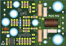
I have tried to rearrange some of the components, out from what you avtech23 and you 00940 have advised me. I have made a picture where there are "components" mounted, I am not sure on how much heat they will produce.
By the way, thanks for making the picture, it was a great help!
avtech23 sorry, I did not write in the right way what I mend about making the traces first. I did understand your advice clearly and as you write now, do I start by placing an important component where I do want it. Then do I make traces, add components, traces and so on
00940 All components are one pole electrolytic caps, as the schematic is showing it should be, I am glad that you do ask and correct that error, as you properly know, do I have about no idea on what I am doing.
Instead of connectors, did I think of just soldering the wires, directly to the board.
About the tighter layout, i.e. R16-Q7, this point was helpful for me, sins it was easier to locate, because it had "a bit of room"
I have tried to redesign those places to accommodate for your changes.
Attachments
Last edited:
- Status
- This old topic is closed. If you want to reopen this topic, contact a moderator using the "Report Post" button.
- Home
- Design & Build
- Construction Tips
- Worst PCB track-layout ever?