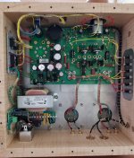
This is a prototype. The builder had some knowledge what he was doing. Dolby SR - Wikipedia
I love this! I'd have it framed and mounted on the wall if SWMBO would ever allow such a thing!!

Friends,
I hope I didn't offense anyone by my writing — I actually did not intend to belittle the soldering skills of the author, but I was rather admiring the virtuosity of the 3-D-ish thing he built. (Well, of course it got colored in tone by the previous post.)
It's amazing how this discussion got intense, pro and contra PCBs / PTP.
I love both methods: Clean PCBs as much as freestyle layouts. (Just like New York City versus Venice, or Florence IT)
PS: Wire-wrap at its best: https://hackaday.com/wp-content/uploads/2014/04/wirewrap.jpg
Last edited:
Looks like they are making wirewrap pens still. I may have to treat myself...
But they‘re quite expensive... ~50.–
WHAT??? No PCB?
This is called "prototyping PCB" or (in Spanish) Placa experimental. It has 20 * 10cm, and holes spaced to match IC pins and small copper pads under it. Obviously when the DUT is ready, I make a PCB for it. See my "High Audio Quality AM Tuner" thread here in DIYAudio some years ago.
Well, not reallyIt's amazing how this discussion got intense, pro and contra PCBs / PTP.
We are talking prototyping here, specifically new design, breaking new ground, etc. , where you do not have a previous idea of the final design, which from pencil drawing on paper to final version will be heavily tweaked and then some.
WHAT PCB will you order if you DO NOT KNOW (yet) the final design?
That anybody suggests that baffles me
Only AFTER you reached your goal you can draw and order a PCB ... and even so it might need some final tweaking.
Even in commercial products now and then you see some added caps (usually for stability) , cut tracks and/or wire jumpers.
Which of course will be included in a later revision.
As of actual production (large or small scale), YES, you WILL draw and use a PCB, nobody in his right mind would offer such kludged products, if anything because of a time waste point of view.
Does anybody think, say, Mr Dolby ever offered multiple copies of his prototype? (although I am certain he carried it as-is to some Recording Studio for Real World testing).
Of course not, all Dolby products I ever saw were built on PCB, what else?
But that at a LATER stage.
Even more, he designed and ordered a CUSTOM IC with his design inside, go figure
How cool is that?
And wirewrap wire. I made some of these ICs on TNT with it. It took forever!Looks like they are making wirewrap pens still. I may have to treat myself...
More practical DIY Interconnect Stuff
But they‘re quite expensive... ~50.–
Maybe electric ones but the manual ones start at around 16 in UK
I should also note that, for the power amp I am currently using, which is one of the superfast Giovanni Stochino designs he specifically notes that his first spin of the PCB was considerably worse in THD performance from his breadboard prototype. I've seen this happen quite a lot. And hands up anyone who has had to deal with the panic when the prototype PCB works great but the first units off the line fail as the buyer has gone to the cheapest supplier who can't control the layup properly.
P.S. I am lousy at deadbugging stuff. It is a skill that needs to be learned
P.S. I am lousy at deadbugging stuff. It is a skill that needs to be learned
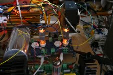
The look and design of a prototype can often be heavily influenced by the resources and budget you have at your disposal. This is all done in my basement lab on near zero budget.
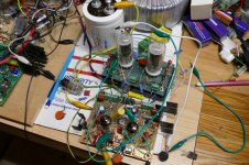
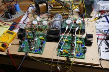
Here is the progression of experiments leading up to what may become another Tubelab board. First off several stupid ideas that I have been playing with for 5 or 6 years came together in the mind of the computer....LTspice. The simulator is pretty good at telling you when an idea WILL NOT work. Determining success and those little details like what it sounds like require a prototype.
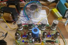
Here several different ideas from the sim get thrown at the workbench in sky-wire style.
Two different output stages were constructed on perf board. The blue one uses 7 or 9 pin tubes, and can be seen extracting 20+ watts from some 50C5 radio tubes. The green one uses 12 pin compactrons and was tested with 6GF5's because they are $1 each. Both were developed with known good Tubelab Universal Driver boards.
Much like the guitar amp in my previous post, the new purpose designed driver stage wan built on top of a failed test board. Note that about half the parts have been ripped out and some new ones sky wired on top.
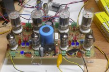
The 6GF5 output stage, and the new driver stage were put together on a one off PC board to prove out the design. It will make 70+ WPC with a regulated 500 volt supply, and 50 WPC with a cheap Antek toroid powering it.
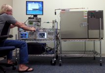
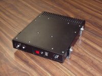
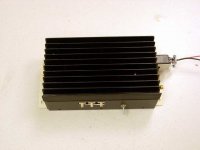
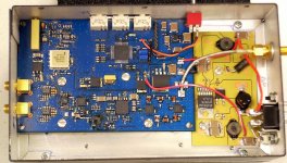
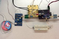
Here is the same progression for a one off prototype I did at Motorola. We had a PCB shop in house, but still some of the individual blocks were reused from other similar projects. This device was just made for a Proof Of Concept. This is where pictures, a words and some test data are used to get a project funded. The "chassis" was a discarded RF power amp that I stripped of it's guts, using only the cabinet and heat sink. (3 pictures)
Here is a picture of a one off prototype. I spent most of a year designing the transmitter, laying out it's PCB, drawing up the details for the chassis, building the only prototype, and taking all the test data. There was a 90 page report that was done detailing all of the progress with data and pictures. I wrote a good chunk of that too......the life of an engineer in the research department of a big company in todays corporate world.
Later on as the company was downsizing and eliminating jobs, our department was absorbed into a larger group, that would eventually be spun off as Freescale, now part of NXP or whoever, today. We were told to generate a "presentation" to justify our jobs to the new bosses. A great panic came over the land. All real work stopped. My friends were in chaos.....
I was not disturbed, and nothing to deal with this issue. They asked.....what's up?, and I replied that I had it covered...…
When "the day" came each one of us was asked to go into a room and give a 10 minute presentation as to why "we" should keep you. There were so many slick slide shows that I couldn't remember who said what. When my turn came, I simply tossed this 12 pound prototype radio out on the table. The big THUD got everyone's attention. I stated that I designed the transmitter, laid out the board, built the prototype, tested it all (TX, RX and data recovery) and wrote the report.....any questions? My unique approach was remembered, and I lived on in that world for 5 more years.
Here the full resources of Motorola were used appropriately. There were dozens of test boards made tested and remade during the initial design cycle. We had an in house PCB shop. I could get a simple 2 layer board in 4 hours. An 4 or more layer board took 1 to 2 days, and a full on 3-4-3 HDI board would take 3 days to a week......want something like 2 layers of Rogers Duroid on 4 layers of FR4, for a 6 layer board....no problem.
We had a full machine shop. I made a simple drawing, and provided the details of each PCB, the internal heat spreaders.....then a mechanical engineer would generate the cad files to mill this chassis out of a single chunk of aluminum. We had a pick and place line to populate SMD boards, Again, someone would take my board files and generate the necessary files for the machines to build our boards. Even though this was a one off proto, several boards were made so that statistical data on the individual circuits could be generated.....all the transmitters were tested in that single chassis for temperature performance.
The Dumm Blonde One testing an LTE transmitter.
Here is the progression of experiments leading up to what may become another Tubelab board. First off several stupid ideas that I have been playing with for 5 or 6 years came together in the mind of the computer....LTspice. The simulator is pretty good at telling you when an idea WILL NOT work. Determining success and those little details like what it sounds like require a prototype.
Here several different ideas from the sim get thrown at the workbench in sky-wire style.
Two different output stages were constructed on perf board. The blue one uses 7 or 9 pin tubes, and can be seen extracting 20+ watts from some 50C5 radio tubes. The green one uses 12 pin compactrons and was tested with 6GF5's because they are $1 each. Both were developed with known good Tubelab Universal Driver boards.
Much like the guitar amp in my previous post, the new purpose designed driver stage wan built on top of a failed test board. Note that about half the parts have been ripped out and some new ones sky wired on top.
The 6GF5 output stage, and the new driver stage were put together on a one off PC board to prove out the design. It will make 70+ WPC with a regulated 500 volt supply, and 50 WPC with a cheap Antek toroid powering it.
Here is the same progression for a one off prototype I did at Motorola. We had a PCB shop in house, but still some of the individual blocks were reused from other similar projects. This device was just made for a Proof Of Concept. This is where pictures, a words and some test data are used to get a project funded. The "chassis" was a discarded RF power amp that I stripped of it's guts, using only the cabinet and heat sink. (3 pictures)
Here is a picture of a one off prototype. I spent most of a year designing the transmitter, laying out it's PCB, drawing up the details for the chassis, building the only prototype, and taking all the test data. There was a 90 page report that was done detailing all of the progress with data and pictures. I wrote a good chunk of that too......the life of an engineer in the research department of a big company in todays corporate world.
Later on as the company was downsizing and eliminating jobs, our department was absorbed into a larger group, that would eventually be spun off as Freescale, now part of NXP or whoever, today. We were told to generate a "presentation" to justify our jobs to the new bosses. A great panic came over the land. All real work stopped. My friends were in chaos.....
I was not disturbed, and nothing to deal with this issue. They asked.....what's up?, and I replied that I had it covered...…
When "the day" came each one of us was asked to go into a room and give a 10 minute presentation as to why "we" should keep you. There were so many slick slide shows that I couldn't remember who said what. When my turn came, I simply tossed this 12 pound prototype radio out on the table. The big THUD got everyone's attention. I stated that I designed the transmitter, laid out the board, built the prototype, tested it all (TX, RX and data recovery) and wrote the report.....any questions? My unique approach was remembered, and I lived on in that world for 5 more years.
Here the full resources of Motorola were used appropriately. There were dozens of test boards made tested and remade during the initial design cycle. We had an in house PCB shop. I could get a simple 2 layer board in 4 hours. An 4 or more layer board took 1 to 2 days, and a full on 3-4-3 HDI board would take 3 days to a week......want something like 2 layers of Rogers Duroid on 4 layers of FR4, for a 6 layer board....no problem.
We had a full machine shop. I made a simple drawing, and provided the details of each PCB, the internal heat spreaders.....then a mechanical engineer would generate the cad files to mill this chassis out of a single chunk of aluminum. We had a pick and place line to populate SMD boards, Again, someone would take my board files and generate the necessary files for the machines to build our boards. Even though this was a one off proto, several boards were made so that statistical data on the individual circuits could be generated.....all the transmitters were tested in that single chassis for temperature performance.
The Dumm Blonde One testing an LTE transmitter.
Attachments
-
 P1000819_x.jpg701.6 KB · Views: 155
 -
 TempTestSetupLargea.jpg148.2 KB · Views: 79
 -
 MVC-012F.JPG211.7 KB · Views: 63
 -
 finisheda.jpg30.5 KB · Views: 75
 -
 Insidea.jpg544.6 KB · Views: 75
 -
 FirstPassTest.jpg103.6 KB · Views: 64
 -
 P1850383_x.jpg569.5 KB · Views: 148
 -
 P1850379_x.jpg548.8 KB · Views: 153
 -
 P1390483_x.jpg689 KB · Views: 151
 -
 P1000891_x.jpg934.1 KB · Views: 151
That thing's nothing more than some slop mess.
And anyone constructing such crap shouldn't have access to a soldering iron.
I don't agree with that at all. How do you learn if you don't build? If you don't build, how do you learn to build?
Often, the builder will cut some square or circular pads from pc stock, and glue those down to the copper foil to make non ground connection points. That addresses some of the concerns about non reliability from parts breaking off ( a valid concern ), and cleans up the appearance. This is an excellent construction technique of long standing.
This was probably a test board on the way to something else.
A similar technique is called manhattan construction, here is a primer:
http://qrpme.com/docs/K7QO Manhattan.pdf
There's a NASA spec for deadbug:
DISCRETE WIRING - DEAD BUGS
There's another weird, really dense and compact point to point with flying leads - "cordwood" ? that I didn't see on that sheet. It was used on the Apollo guidance computers that went into space.
I think.
Apollo, yeah
Apollo! YESS!
An Apollo Spacecraft Computer Is Brought Back to Life - WSJ
Apollo Guidance Computer: Dipstiks and reverse engineering the core rope simulator
what‘s even more intriguing is the rope core memory, but this is totally another story...
Apollo guidance computers
I think.
Apollo! YESS!
An Apollo Spacecraft Computer Is Brought Back to Life - WSJ
Apollo Guidance Computer: Dipstiks and reverse engineering the core rope simulator
what‘s even more intriguing is the rope core memory, but this is totally another story...
Last edited:
....Does anybody think, say, Mr Dolby ever offered multiple copies of his prototype? (although I am certain he carried it as-is to some Recording Studio for Real World testing)....
I strongly suspect he had his own in-house listening facility. Maybe even with wires to his workbench. So it probably traveled little or not at all. It's just too floppy. And it may just be one or two channels of SR, while Studios used Dolby modules 16 and 24 at a time.
When I did a much smaller build, I had a 99% good idea where I was going, and built it to stand travel. Last step of the build I realized I had a major mis-match. (An early change of power-plan not fully thought-forward to meter level.) So there was a little converter board tucked on the side. In haste, to expedite testing and use. I knew it had a flaw which might not matter so I left it "temporary". Over the next few gigs I decided the flaw was acceptable so I just re-did wires and mounts; but I could have torn it out and installed a more complex fix.
He would also, in that day, have his own PCB facility (in-house or local fab). So when the proto-flop was shown to be no flop, he'd have it copied to PCB and stuffed. Ideally crunched-down to fit in the standard Dolby-module socket; but an intermediate step would be a larger box with flying cables to a rack socket. As you later say, by stages he reduced all that to mostly one custom chip. And as you say, he needed multiple iterations that he could modify quickly before committing to an un-changable chip.
... and I replied that I had it covered...…
Thanks for sharing!
Cool to see the progress of a project from a messy thing into a finished thing!
I think you got a cool profession.
Yes, PCB is neat but almost completely inflexible. None of my projects ever go to PCB, unless you count Veroboard as PCB.
I always struggled with valve point to point layouts.
At least a pcb is annotated so you know which component on the diagram you are looking at.
I watch in awe as Marshall production line staff put together point to point systems.
I have never had a good memory so probably explains why I struggle with p2p.
Ugly style construction works great for prototyping, and believe it or not it's considerably cleaner than what I often do for testing.
In testing my 0-500V 500mA power supply I clamped a bunch of FETs to a block of aluminum, then wired it up "flying lead" style. It was extremely ugly, but when testing a new design I find that it works well. Once I had it working the way I wanted, I updated my schematic and designed a PCB.
Also, for vacuum tube circuits I really like point-to-point. I've never liked PCB mounted tube sockets. In my opinion it puts too much heat and mechanical stress on the PCB (especially some new 9-pin sockets that have a death grip on tubes).
We all have to start somewhere I suppose...
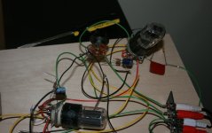
"Dead bug" is exactly where I started. That's the method I used in the first picture below, which is some sort of 6SN7 stereo preamp I cobbled together about two decades ago. Oddly enough it was tolerably quiet despite the lack of a chassis. Heck, none of it was even attached to the board; the whole web o' death was just lying there making music. Now that I think of it, it looks more like roadkill than dead bugs (yes, this is dangerous; however there is an isolated power supply to the left of the frame).
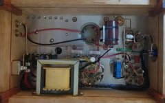
The second picture shows my progress as I wised up and began combining machine work and crapentry to create real chassis (chasseez...cheeses... whatever). This is one of a pair of monoblocks from a Vinylsavor design I did as a point-to-point build with 1920's-style ground buses. They're dead silent. Btw, monoblocks are more than twice the work - particularly so if one chooses to build them as mirror images.
The last image is the underside of a Tubelab SEII completed about six months ago. I'd never previously built a tube amp from a PC board, and I'll admit this threw me for a loop. I had the bare board up and running in four hours; another four hours and I had it on a suitable breadboard for further testing. But... designing and machining the chassis, incorporating the remote volume control and lacing the cables took another six weeks.
"Dead bug" is exactly where I started. That's the method I used in the first picture below, which is some sort of 6SN7 stereo preamp I cobbled together about two decades ago. Oddly enough it was tolerably quiet despite the lack of a chassis. Heck, none of it was even attached to the board; the whole web o' death was just lying there making music. Now that I think of it, it looks more like roadkill than dead bugs (yes, this is dangerous; however there is an isolated power supply to the left of the frame).
The second picture shows my progress as I wised up and began combining machine work and crapentry to create real chassis (chasseez...cheeses... whatever). This is one of a pair of monoblocks from a Vinylsavor design I did as a point-to-point build with 1920's-style ground buses. They're dead silent. Btw, monoblocks are more than twice the work - particularly so if one chooses to build them as mirror images.
The last image is the underside of a Tubelab SEII completed about six months ago. I'd never previously built a tube amp from a PC board, and I'll admit this threw me for a loop. I had the bare board up and running in four hours; another four hours and I had it on a suitable breadboard for further testing. But... designing and machining the chassis, incorporating the remote volume control and lacing the cables took another six weeks.
Attachments
- Status
- This old topic is closed. If you want to reopen this topic, contact a moderator using the "Report Post" button.
- Home
- Design & Build
- Construction Tips
- Is this supposed to work?