Yes, that´s the one.I don't know what JMFahey used, but there's a free Photoshop-like program named Gimp, but like Photoshop it has lots of features and thus a longer learning curve than MS Paint or Irfanview. I use Gimp mostly to crop and resize photos, and it took some time to find the right tools on it just to do that.
ETA: Inkscape is a whole different type of tool - it's vector based and comparable to Adobe Illustrator. It's not what you want to use to manipulate a bitmap image.
Wasn´t sure which is which so I enclosed Inkscape between interrogation marks
")
As mentioned, personally use Paint Shop Pro since Windows 3.1 days
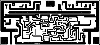
@ Arnold Ziffel: I bet you didn´t sleep all night editing that PCB dot by dot
, congratulations.You still need the polishing stage of drawing little white circles at each drill hole, so when etched they serve as drill tip centering guides ... or you´ll have a bitter experience of needle thin drills wandering all over the place, either placing holes "anywhere but where you need them"
or plain breaking them.Something like this:
Attachments

Good advice!You still need the polishing stage of drawing little white circles at each drill hole, so when etched they serve as drill tip centering guides ... or you´ll have a bitter experience of needle thin drills wandering all over the place, either placing holes "anywhere but where you need them"
If it were my PCB project, I'd likely try using the toner image 'as-is', though it's always better to have the enlarged circles (solder pads) around the drilled holes. There are some small marks which will show where the holes should go.
With my drilling setup (high speed Dremel in a 'drill press, carbide bit) I can drill holes without an 'indexing mark'.
A slower drill speed, different drill, and more pressure would probably cause wandering problems.
Good work on the image re-work!
I use an old copy of Photoshop Elements -which came free with a scanner years ago- for work like this.
See attached file. It's a reconstruction of the printed layout under a PCB software. No check was made to the circuit or the BOM file.
You can use the Sprint Layout viewer (free - FREE VIEWER SOFTWARE, ELECTRONIC-SOFTWARE-SHOP) to print.
You can use the Sprint Layout viewer (free - FREE VIEWER SOFTWARE, ELECTRONIC-SOFTWARE-SHOP) to print.
Attachments
jpr_pt,
That's great!
Thank you so much!
How did you do that? It took about 8 hours of idiotic editing in MS Paint and my image looks awful.
I think it would be very helpful for others to know how you did this. I've seen lots of posts with images of PCBs with top and bottom layers, but no gerbers, or the like.
Thank you again.
Thank you all -az
Hi,
I’m going to build an amp based on the Douglas Self and Randy Slone’s designs form buildaudioamps.com, (http://buildaudioamps.com/project-61/).
The designer has an image of the PCB that has both the foil and component graphics. I just want the foil side. I’m not an expert manipulating images to make a PCB.
Is there a standard or easy method to isolate the layers so I can use the image to make a PCB?
I’ve attached the image.
Thank you for your advice - az
If you can find a software that can remove a single color.
But then you still have the scaling problem.
jpr_pt,
That's great!
Thank you so much!
How did you do that? It took about 8 hours of idiotic editing in MS Paint and my image looks awful.
I think it would be very helpful for others to know how you did this. I've seen lots of posts with images of PCBs with top and bottom layers, but no gerbers, or the like.
Thank you again.
Thank you all -az
It took me about 1 hour to do it. I used the Sprint Layout software. It allows to read a picture file. I took the file from the site you indicated and scaled to the 6x2.725" size. Then overlap the components and draw the connections. If you use the full version you can export the gerber and drill files that allows you to place an order on a PCB manufacture.
I gave up of doing my own pcb at home. It's a mess. There's a lot of manufacters doing that, with the advantage of double face (plated holes). The main drawback is the delivery time
You guys are amazing!
Thank you so much jpr_rt and Gunni!
You are so incredibly generous.
I have a lot to learn about creating PCBs. I've spent most of my electronic history soldering kit boards or resorting to point-to-point.
I'll try to find a PCB maker as you have advised.
Thank you again so much!
I wish you all a wonderful holiday and great new year - az
- Status
- This old topic is closed. If you want to reopen this topic, contact a moderator using the "Report Post" button.
- Home
- Design & Build
- Construction Tips
- How do I isolate the layers form an image to make a PCB?