This paper is also interesting, did read this a long time ago, contains very usefull info.
https://www.hobbielektronika.hu/forum/getfile.php?id=253790
https://www.hobbielektronika.hu/forum/getfile.php?id=253790
Things such as...
https://www.hobbielektronika.hu/forum/getfile.php?id=253790
With 4 foot long equations tend to make me run a mile. I have looked elsewhere for information about your topology and there are claims that the available closed loop bandwidth is improved by factors of N where N are the number of levels. I would be wary about the interpretation of such claims.
In the above paper reference is made to Feed Forward. As far as I can see this is Pre-Filter Feedback so why not call it Pre-Filter Feedback? I do not have a model for your topology and am uncertain that I could recreate it. In particular the manner in which the flying capacitors are charged/recharged. That might happen as a matter of course during operation.
If you could provide such a base LTSpice model, .asc file, I would be happy to have a play. Failing that you might consider the following but bear in mind that it might be incomplete or slightly incorrect.
You suggest that the distortion performance of such a topology is worse as a result of the added switching nodes. You should be able to use Pre Filter Feedback to improve that as follows.
Let's say you have a Section operating frequency of Fs and a Total operating frequency of Ft (N.Fs). As I suggest I do not believe that with Post Filter Feedback you can exceed a crossover frequency of Fs/PI. However with Pre Filter Feedback a crossover frequency for that particular loop of Ft/PI should be realisable.
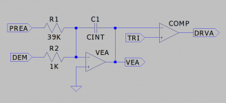
Consider the first picture. This is standard practice for Pre Filter Feedback. Values are nominal and the value for CINT is omitted. You calculate CINT such that the slope of the integrated output square wave matches the slope of the modulator triangle wave. At zero output the triangle at VEA is half the amplitude of the modulator triangle.
Under those conditions the loop crosses over at Fs/Pi. Single section.
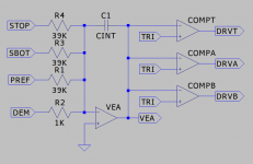
In your half bridge, three level[?], instance at first sight things look slightly complicated due to the level shifts involved but it would appear that such shifts, top to bottom, will cancel. It also appears to be the case that the averaged outputs, top and bottom, are half of the main summed output.
Assuming this is the case then you can proceed with the second picture. CINT does not change. You just add in the extra resistors and comparators. You may wish to consider adding a DC servo around this section should you find that the Top/Bottom DC offset match is not precise. I would guess that would be unlikely.
Having become inconsistent. Switch Top, STOP, Switch Mid, SMID, Switch Bottom, SBOT and Drive Top, DRVT, Drive Mid, DRVM, and Drive Bottom, DRVB.
Assuming my suggestion about scaling is correct then the new resistors will have the same values as the original one. In the half bridge case your new crossover frequency becomes 2Fs/PI. Again this is strictly Pre Filter.
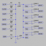
This is extended to your full bridge case in the third picture. Again I am slightly losing the plot over labelling but Switch Left Top, Mid, Bottom. Switch Right Top, Mid, Bottom and similar with the comparator outputs. Then whatever with the triangle waves.
Also just in case when I refer to Switch I am really referring to the associated switched nodes.
Again all component values remain the same. You just add some more resistors and comparators. This time your crossover frequency becomes 4Fs/PI or Ft/PI. Once complete then the closed loop response, DEMand to Pre Filter Output for the values chosen is 39 Volts per Volt.
At this point you can add the Post Filter Ouput Feedback around this internal loop as proposed in your other paper...
https://www.meng-engineering.ch/_download/Mathcad%20-%20Postfilter-Feedback-Halfbridge-Single-Supply-170V.pdf
This also tries to introduce four foot long equations but the simple solution is to mess about in Spice. The fourth picture shows a 40KHz cutoff filter scaled for a 4R load, yes speakers are not but. E1 represents the previously designed internal loop with a gain of 39 Volts per Volt. It is ideal but all you care about is that it crosses over, runs out of steam, at Ft/PI and you, almost, don't care about that because your external loop is going to be limited to Fs/PI.
Plotting the control to output response you find out where the -7dB point is. That's because we are going to introduce a phase bump, similar to your paper, of 7dB in the external loop to cancel one of the filter poles. In this case it is at 375KHz. Your section switching frequency is 240KHz so your maximum loop crossover is 240K/PI or 76KHz. That sets the gain in the external loop at this frequency as (76/375)^2 or 0.04, at the moment the response is second order hence the squared term.
We end up with the fifth picture. Here I have used the trick of breaking the loop with VAC and plotting V(a)/V(b) to get the loop behaviour and -7dB point. R1, standard value, is low and we do not precisely hit 76KHz. Such is life and other things may matter more.
Now we add the phase bump as in the sixth picture. It involves attenuating the low frequency gain by a factor of five so we also have to increase the error amplifier gain by the same factor to bring things back. The capacitor value is chosen to have an impedance of 13K5 at the desired frequency of 76KHz.
The point... If we unload the filter as shown in the seventh picture then crossover is still occurring with 42 degrees phase margin as a result of the added phase bump and therefore we hope that the system is still stable.
We also get to nominally break the DC path, add a pole, around the error amplifier as shown in the eighth picture to improve the low frequency performance. In this case at about 40KHz but caveats here and elsewhere.
The almost don't care in respect of ignoring Ft/PI given you are limited to Fs/PI assumes the closed internal loop will not contribute phase shifts to the external loop. For Ft = 4Fs that assumption might be valid. Ft = 2Fs probably not. Also breaking the external loop as mentioned above robs phase margin.
Then you get into the wonderful world of clamping or limiting error amplifiers when the loop loses the plot in order to help it gracefully find its way back again.
Now I'll try to add the right pictures in the right order. Just a moment. Hopefully that works.
...
https://www.hobbielektronika.hu/forum/getfile.php?id=253790
With 4 foot long equations tend to make me run a mile. I have looked elsewhere for information about your topology and there are claims that the available closed loop bandwidth is improved by factors of N where N are the number of levels. I would be wary about the interpretation of such claims.
In the above paper reference is made to Feed Forward. As far as I can see this is Pre-Filter Feedback so why not call it Pre-Filter Feedback? I do not have a model for your topology and am uncertain that I could recreate it. In particular the manner in which the flying capacitors are charged/recharged. That might happen as a matter of course during operation.
If you could provide such a base LTSpice model, .asc file, I would be happy to have a play. Failing that you might consider the following but bear in mind that it might be incomplete or slightly incorrect.
You suggest that the distortion performance of such a topology is worse as a result of the added switching nodes. You should be able to use Pre Filter Feedback to improve that as follows.
Let's say you have a Section operating frequency of Fs and a Total operating frequency of Ft (N.Fs). As I suggest I do not believe that with Post Filter Feedback you can exceed a crossover frequency of Fs/PI. However with Pre Filter Feedback a crossover frequency for that particular loop of Ft/PI should be realisable.
Consider the first picture. This is standard practice for Pre Filter Feedback. Values are nominal and the value for CINT is omitted. You calculate CINT such that the slope of the integrated output square wave matches the slope of the modulator triangle wave. At zero output the triangle at VEA is half the amplitude of the modulator triangle.
Under those conditions the loop crosses over at Fs/Pi. Single section.
In your half bridge, three level[?], instance at first sight things look slightly complicated due to the level shifts involved but it would appear that such shifts, top to bottom, will cancel. It also appears to be the case that the averaged outputs, top and bottom, are half of the main summed output.
Assuming this is the case then you can proceed with the second picture. CINT does not change. You just add in the extra resistors and comparators. You may wish to consider adding a DC servo around this section should you find that the Top/Bottom DC offset match is not precise. I would guess that would be unlikely.
Having become inconsistent. Switch Top, STOP, Switch Mid, SMID, Switch Bottom, SBOT and Drive Top, DRVT, Drive Mid, DRVM, and Drive Bottom, DRVB.
Assuming my suggestion about scaling is correct then the new resistors will have the same values as the original one. In the half bridge case your new crossover frequency becomes 2Fs/PI. Again this is strictly Pre Filter.
This is extended to your full bridge case in the third picture. Again I am slightly losing the plot over labelling but Switch Left Top, Mid, Bottom. Switch Right Top, Mid, Bottom and similar with the comparator outputs. Then whatever with the triangle waves.
Also just in case when I refer to Switch I am really referring to the associated switched nodes.
Again all component values remain the same. You just add some more resistors and comparators. This time your crossover frequency becomes 4Fs/PI or Ft/PI. Once complete then the closed loop response, DEMand to Pre Filter Output for the values chosen is 39 Volts per Volt.
At this point you can add the Post Filter Ouput Feedback around this internal loop as proposed in your other paper...
https://www.meng-engineering.ch/_download/Mathcad%20-%20Postfilter-Feedback-Halfbridge-Single-Supply-170V.pdf
This also tries to introduce four foot long equations but the simple solution is to mess about in Spice. The fourth picture shows a 40KHz cutoff filter scaled for a 4R load, yes speakers are not but. E1 represents the previously designed internal loop with a gain of 39 Volts per Volt. It is ideal but all you care about is that it crosses over, runs out of steam, at Ft/PI and you, almost, don't care about that because your external loop is going to be limited to Fs/PI.
Plotting the control to output response you find out where the -7dB point is. That's because we are going to introduce a phase bump, similar to your paper, of 7dB in the external loop to cancel one of the filter poles. In this case it is at 375KHz. Your section switching frequency is 240KHz so your maximum loop crossover is 240K/PI or 76KHz. That sets the gain in the external loop at this frequency as (76/375)^2 or 0.04, at the moment the response is second order hence the squared term.
We end up with the fifth picture. Here I have used the trick of breaking the loop with VAC and plotting V(a)/V(b) to get the loop behaviour and -7dB point. R1, standard value, is low and we do not precisely hit 76KHz. Such is life and other things may matter more.
Now we add the phase bump as in the sixth picture. It involves attenuating the low frequency gain by a factor of five so we also have to increase the error amplifier gain by the same factor to bring things back. The capacitor value is chosen to have an impedance of 13K5 at the desired frequency of 76KHz.
The point... If we unload the filter as shown in the seventh picture then crossover is still occurring with 42 degrees phase margin as a result of the added phase bump and therefore we hope that the system is still stable.
We also get to nominally break the DC path, add a pole, around the error amplifier as shown in the eighth picture to improve the low frequency performance. In this case at about 40KHz but caveats here and elsewhere.
The almost don't care in respect of ignoring Ft/PI given you are limited to Fs/PI assumes the closed internal loop will not contribute phase shifts to the external loop. For Ft = 4Fs that assumption might be valid. Ft = 2Fs probably not. Also breaking the external loop as mentioned above robs phase margin.
Then you get into the wonderful world of clamping or limiting error amplifiers when the loop loses the plot in order to help it gracefully find its way back again.
Now I'll try to add the right pictures in the right order. Just a moment. Hopefully that works.
...
Attachments
-
 Screenshot from 2019-08-25 10-40-56.png23.4 KB · Views: 616
 -
 Screenshot from 2019-08-25 10-58-31.png36.9 KB · Views: 593
 -
 Screenshot from 2019-08-25 11-21-47.png38.7 KB · Views: 609
 -
 Screenshot from 2019-08-25 12-28-10.png59.3 KB · Views: 607
 -
 Screenshot from 2019-08-25 12-45-26.png61.3 KB · Views: 597
 -
 Screenshot from 2019-08-25 13-01-58.png60.4 KB · Views: 172
 -
 Screenshot from 2019-08-25 13-16-23.png63.1 KB · Views: 159
 -
 Screenshot from 2019-08-25 13-20-51.png43.7 KB · Views: 166
Hi orbitfractal.
First I have I have from reading, so the answers or this is better or not is from papers not mine, what I do is play with it and try to improve.
However with multilevel, we have the issue that fase is important to stay into the multiplication factor and keep multilevel switching, I havd done from three to 8, but it get pretty complicated with more levels, I stick on max 5 with two three levels bridget and 90 degree shift between, that makes a 5 level with less complicated circuit.
I have afcourse the need of A good driver ic for the mosfets, or a good discrete schematic, I do not now if the multilevel switching has inpact on the upper fet who needs to have a voltage pump, this pump do not switch when that fet is not active in a multilevel, but maybe I am wrong, there chips who does 5 level and it works.
Do I see right you do feedback from every level? and sum it?
I like discrete, can play more then.
Here a two .asc to play with, and have fun, if you have not some models ask me I will send.
regards
Attachments
Last edited:
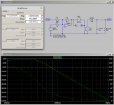
Here's my attempt at your half bridge.
You'll notice that my model is very much simplified and, for the moment just includes the proposed Pre Filter Feedback. I was more than surprised when it worked first time.
My original suggestion as to scaling of resistors was slightly wrong. You have to ratio them 2:1. I hacked the slope matching in Spice as well.
The performance looks a bit dirt. Maybe I got something wrong but...
Have a poke about.
Attachments
Here's my attempt at your half bridge.
You'll notice that my model is very much simplified and, for the moment just includes the proposed Pre Filter Feedback. I was more than surprised when it worked first time.
My original suggestion as to scaling of resistors was slightly wrong. You have to ratio them 2:1. I hacked the slope matching in Spice as well.
The performance looks a bit dirt. Maybe I got something wrong but...
Have a poke about.
Thanks for the help, Do you now a good mosfet driver ic for use with multilevel? I have some worries about the bootstrap circuit when I get multilevel, is it fast enough to provide the voltages in such a ic, I think it works because more people are use them in inverters.
Thanks for the help, I go simplify also the system, using models in stead of complete ic,s. You have clearly much more experience with LTspice then me, and learn it at mine age 62 takes longer as normal.
I do now the circlotron who starts again when weather get less hot, sitting behind a soldering iron with 32 degrees is hot, like today, so it is fall project (hybrid amp, autobias).
Your design do the same, the multilevel switching get bad with feedback and a extra faseshift that it cause, only the multilevel btl with slef oscillation do work, the faseshift is because the triangles do not get changed, maybe a faseshifting there can repair the switching, with self oscillating it do that automatically and do multiplying the frequency.
I have included the feedbacked self oscilating type, probe the resistor on the output before the filter to see it.
Stil it is that feedback multilevel is not that easy except self osc types until three level noth higher.
regards
Attachments
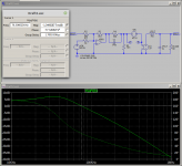
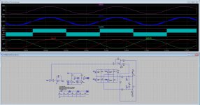
Here I have test with cascade stages, this does better and is open loop already nice.
Do you setup your schematic for deadtime?
When you try it, set the opamps vack because I had use models, and you did universal, need fast opamps. First plot op pic is openloop test, rest is feedback with two integrators.
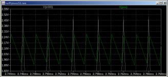
What means the numbers between brackets into the ltspice harmonic distortion plot. And why I have such a lot 3th harmonics? deatime maybe?.
regards
Do you setup your schematic for deadtime?
When you try it, set the opamps vack because I had use models, and you did universal, need fast opamps. First plot op pic is openloop test, rest is feedback with two integrators.
What means the numbers between brackets into the ltspice harmonic distortion plot. And why I have such a lot 3th harmonics? deatime maybe?.
regards
Attachments
Last edited:
What means the numbers between brackets into the ltspice harmonic distortion plot.
There was a long thread (initiated by myself in September 2014) about the second THD figure in brackets in the Yahoo LTspice users' group: Yahoo! Groups
The consensus seemed to be that the second, bracketed, figure is THD for all harmonics, compared to the first, which is for the specified number of harmonics, or for 9 harmonics if not specified.
For example, I have just run four .four analyses on a circuit:
.four 1k 10 V(out) yields 0.001468%(0.013915%);
.four 1k 100 V(out) yields 0.003776%(0.014504%);
.four 1k 1000 V(out) yields 0.014494%(0.014507%);
.four 1k 10000 V(out) yields 0.014505%(0.014518%).
These figures would tend to confirm the conjecture that the bracketed figure is THD for all harmonics. There are, however, minor inconsistencies to be aware of. For example, in this example, why are the four bracketed figures not identical?
In the case of your circuit, you have only measured THD for six harmonics. The fact that the bracketed figure is so much higher than the first suggests that there is substantial distortion showing with high harmonics, though I wouldn't like to comment on whether distortion at such high frequencies is audible or not.

Hi all
I have now get 10 x 20124s ic, but when I do simulate it, I have the model, it looks it goes into protection mode when I have 65 volt rails on mosfets, with 35 volts it works, OC resistors? when I do the 12 volts on the chip through ground and not the -65 reference then it works also. I have also uge shoot through I do something wrong and need a solution before the pcb starts. I have now 3 projects Or the model is just wrong and need real live design.
something to do with the OC inputs? do somebody now to correct this.
thanks.
kees
I have now get 10 x 20124s ic, but when I do simulate it, I have the model, it looks it goes into protection mode when I have 65 volt rails on mosfets, with 35 volts it works, OC resistors? when I do the 12 volts on the chip through ground and not the -65 reference then it works also. I have also uge shoot through I do something wrong and need a solution before the pcb starts. I have now 3 projects
Or the model is just wrong and need real live design.something to do with the OC inputs? do somebody now to correct this.
thanks.
kees
Attachments
Last edited:
Hi all
I have now get 10 x 20124s ic, but when I do simulate it, I have the model, it looks it goes into protection mode when I have 65 volt rails on mosfets, with 35 volts it works, OC resistors? when I do the 12 volts on the chip through ground and not the -65 reference then it works also. I have also uge shoot through I do something wrong and need a solution before the pcb starts. I have now 3 projects
something to do with the OC inputs? do somebody now to correct this.
thanks.
kees
I have found the error, the bootstrap diode was to slow, I did need a fast recovery type, then it does work.
First all have a happy new year.
For the people who think I am dead, that is not the case, but mine stepfather did die, has cancer and is passing away in 5 days after discovering, weight did go down from 128 kilo to 51 kilo, the pic did let see a horror movie, he was become a zombie.
Because of that an that I need to help mother does make that I am not very active, mother is 88 and I need to help her. Now it is a while ago, new year start and have started to remove some more hobbies, I had to much projects I have now sell that stuff and keep busy with electronics.
For the amps, I have desided to go into class D and hybrids in circlotron vorm, the class d go first because of the learnfase.
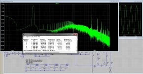
I have now find nice calculation program on internet Mathpapa Mathpapafault.jpg is to let see this site does correct and advice also, nice.
Equation Solver - MathPapa
There I can fill in firmula,s as it is written by most designers and professors, nice stuff helps a lot.
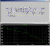
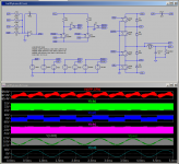
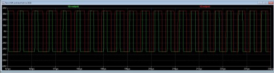
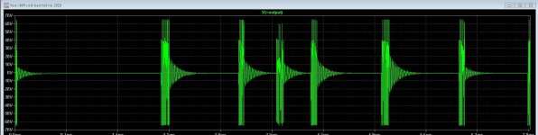
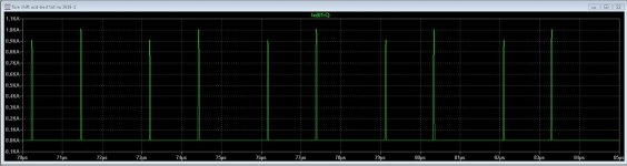
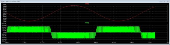
For the class d I have done now with the UC20124s ic,s does very nice in multilevel, have post and prefeedback with faseshift network.
Pic,s are the calculator and the sims.
By the way what is happened with Mueta BV? this company is very close to where I live, do not answer phone, it is closed.
For the people who think I am dead, that is not the case, but mine stepfather did die, has cancer and is passing away in 5 days after discovering, weight did go down from 128 kilo to 51 kilo, the pic did let see a horror movie, he was become a zombie.
Because of that an that I need to help mother does make that I am not very active, mother is 88 and I need to help her. Now it is a while ago, new year start and have started to remove some more hobbies, I had to much projects I have now sell that stuff and keep busy with electronics.
For the amps, I have desided to go into class D and hybrids in circlotron vorm, the class d go first because of the learnfase.
I have now find nice calculation program on internet Mathpapa Mathpapafault.jpg is to let see this site does correct and advice also, nice.
Equation Solver - MathPapa
There I can fill in firmula,s as it is written by most designers and professors, nice stuff helps a lot.
For the class d I have done now with the UC20124s ic,s does very nice in multilevel, have post and prefeedback with faseshift network.
Pic,s are the calculator and the sims.
By the way what is happened with Mueta BV? this company is very close to where I live, do not answer phone, it is closed.
Attachments


There was a long thread (initiated by myself in September 2014) about the second THD figure in brackets in the Yahoo LTspice users' group: Yahoo! Groups
The consensus seemed to be that the second, bracketed, figure is THD for all harmonics, compared to the first, which is for the specified number of harmonics, or for 9 harmonics if not specified.
For example, I have just run four .four analyses on a circuit:
.four 1k 10 V(out) yields 0.001468%(0.013915%);
.four 1k 100 V(out) yields 0.003776%(0.014504%);
.four 1k 1000 V(out) yields 0.014494%(0.014507%);
.four 1k 10000 V(out) yields 0.014505%(0.014518%).
These figures would tend to confirm the conjecture that the bracketed figure is THD for all harmonics. There are, however, minor inconsistencies to be aware of. For example, in this example, why are the four bracketed figures not identical?
In the case of your circuit, you have only measured THD for six harmonics. The fact that the bracketed figure is so much higher than the first suggests that there is substantial distortion showing with high harmonics, though I wouldn't like to comment on whether distortion at such high frequencies is audible or not.
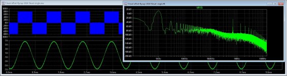
This distortion do not show up in the plot itself?, that is little weird. But maybe I do wrong understanding LTspice.
I ran the .asc file you posted in #147, and it was still running after 56 minutes! Either you have a lot of patience or a very fast computer - my own computer, like myself, is somewhat on the slow side...
Anyway, I added a few commands to your file, which both increase the accuracy and reduce the running time to around 30 seconds. The parameter fft can be adjusted to increase accuracy at the expense of time - if fft=2**20 the sim takes arund 90 seconds but the accuracy is increased - but it only makes a small difference to the .four result. The file is posted below.
Just to avoid any confusion, the figures I quoted are not those of your circuit, but from another circuit of my own. The intention was simply to show that the greater the number of harmonics included in a .four analysis, the closer the two distortion figures are. This was in response to your question about why there are two THD figures given in a .four analysis, with a higher second figure in brackets.
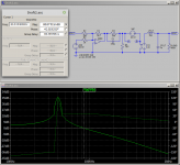
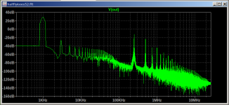
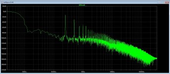
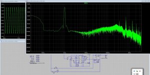
In the case of your circuit, and referring to the third image in post #147, the Error Log shows distortion of c. 0.0019% measuring the first six harmonics only. The fft plot shows that the first six harmonics are indeed at a low level.
There are, however, artefacts of the switching frequency showing at a much higher level at c. 600kHz and above, and these are the reason why the second distortion figure (in brackets) is much higher, c. 0.62%.
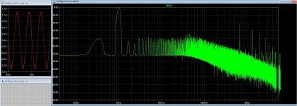
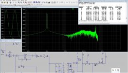
What I can see is that the even harmonics are at a very low level, hidden beneath the noise floor, and the odd harmonics are at a higher level than the evens. I can't see that the 3rd harmonic is at a high level compared to the other odd harmonics.
I'm sure you are aware that a harmonic profile like this would typically be associated with a symmetrical circuit.
Anyway, I added a few commands to your file, which both increase the accuracy and reduce the running time to around 30 seconds. The parameter fft can be adjusted to increase accuracy at the expense of time - if fft=2**20 the sim takes arund 90 seconds but the accuracy is increased - but it only makes a small difference to the .four result. The file is posted below.
This distortion do not show up in the plot itself?, that is little weird. But maybe I do wrong understanding LTspice.
Just to avoid any confusion, the figures I quoted are not those of your circuit, but from another circuit of my own. The intention was simply to show that the greater the number of harmonics included in a .four analysis, the closer the two distortion figures are. This was in response to your question about why there are two THD figures given in a .four analysis, with a higher second figure in brackets.
In the case of your circuit, and referring to the third image in post #147, the Error Log shows distortion of c. 0.0019% measuring the first six harmonics only. The fft plot shows that the first six harmonics are indeed at a low level.
There are, however, artefacts of the switching frequency showing at a much higher level at c. 600kHz and above, and these are the reason why the second distortion figure (in brackets) is much higher, c. 0.62%.
And why I have such a lot 3th harmonics?
What I can see is that the even harmonics are at a very low level, hidden beneath the noise floor, and the odd harmonics are at a higher level than the evens. I can't see that the 3rd harmonic is at a high level compared to the other odd harmonics.
I'm sure you are aware that a harmonic profile like this would typically be associated with a symmetrical circuit.
Attachments
I ran the .asc file you posted in #147, and it was still running after 56 minutes! Either you have a lot of patience or a very fast computer - my own computer, like myself, is somewhat on the slow side...
Anyway, I added a few commands to your file, which both increase the accuracy and reduce the running time to around 30 seconds. The parameter fft can be adjusted to increase accuracy at the expense of time - if fft=2**20 the sim takes arund 90 seconds but the accuracy is increased - but it only makes a small difference to the .four result. The file is posted below.
Just to avoid any confusion, the figures I quoted are not those of your circuit, but from another circuit of my own. The intention was simply to show that the greater the number of harmonics included in a .four analysis, the closer the two distortion figures are. This was in response to your question about why there are two THD figures given in a .four analysis, with a higher second figure in brackets.
In the case of your circuit, and referring to the third image in post #147, the Error Log shows distortion of c. 0.0019% measuring the first six harmonics only. The fft plot shows that the first six harmonics are indeed at a low level.
There are, however, artefacts of the switching frequency showing at a much higher level at c. 600kHz and above, and these are the reason why the second distortion figure (in brackets) is much higher, c. 0.62%.
What I can see is that the even harmonics are at a very low level, hidden beneath the noise floor, and the odd harmonics are at a higher level than the evens. I can't see that the 3rd harmonic is at a high level compared to the other odd harmonics.
I'm sure you are aware that a harmonic profile like this would typically be associated with a symmetrical circuit.
This I am aware of.
I'm sure you are aware that a harmonic profile like this would typically be associated with a symmetrical circuit. Also the dead time is quite of influence of that 3th harmonic, maiking that tight that thrith get under -110dB.
Your writing was clear, and it was a question why the second between brackets are for, now you have explane that I do not why, it it is from the higher 600 Khz then it is not of concern for me, the design is a three level and it does also double the carrier maybe also here is a reason for that plot.
I do now that is not for mine schematic I had some questions about that second plot I did not find, but have info now thanks.
Thanks for the reaction, and do now, I am not a LTspice professor, I do not know much only the basic stuf.
regards
Last edited:
OK Kees
Good luck with your design!
You did simplify the schematic for faster sims, and this needs some skills for ltpspice you have and I not,, but for this I have a fast i7x pc with much memory, it does still some slower work than your work but I have the time of the world, and that feels quite relaxed.
Now I am busy with stop some projects and sell them beause I had much to much and nothing came out of mine hands, this is a problem I not only have, a lot of diy people has this problem I presume.
regards
Hi everyone. I have just joined this forum but have been reading the posts for a couple of weeks. I have a Mac mini music server and need a decent amp to plug it in. I could buy a Yamaha WXA-50 or build something myself. Here is a list of the main components I would use:
Wondom AA-AB32512
Mean Well RPS-500-36
Stereo Stepped ladder attenuator 10K
DAC Khadas Tone Board mounted inside case
Case 1455T2201
Panel mount usb c extension cable
2x Speaker Terminals
2x RCA sockets
IEC socket with switch
Selector switch double pole toggle
Knob
The WXA-50 and these components cost about the same. Would the DIY amp be worth building?
This distortion do not show up in the plot itself?, that is little weird. But maybe I do wrong understanding LTspice.
I can't give a specific example but something I am working on at the moment throws up an indication as to the cause of the nature of your plots not showing the distortion components.
My circuit incorporates a DC servo and if I do not allow time for it to settle prior to commencing logging of data, for example .tran 15m 10m 1n uic, the low frequency result in the FFT shows the same slopes either side of the 1KHz test tone.
Your circuits include a number of large value flying capacitors that are likely to produce such and effect in that it will/may take some time to acquire the correct average, DC, operating voltage.
I have noticed that in your .tran statements you appear to regularly miss of the .uic, Use Initial Conditions, directive. As a result the analyser tries to guess an initial DC operating point which it is likely to get wrong and also spends a lot of time trying to get it wrong.
That also appears to hurt the speed of the subsequent transient analysis.
For switching circuits such as this I always include the uic directive and in the rare cases where it loses the plot I will include IC statements for the suspect components. Generally those will be inductors and capacitors.
For a capacitor CTRL Right click and in one of available lines add IC=200V. If that is the wrong way up rotate the capacitor the other way or use IC=-200V. Make sure that uic is checked in the transient statement.
@ElliJ
Building something that will work as comfortable, reliable and well as the Yamaha is hard to do from your chosen parts. If you want a perfect result, go for the WXA-50.
If you want to spent time while building something with unspecific result, which is called "a hobby", buy parts...
It depends on you, your tools, skills and patience.
- Home
- Amplifiers
- Class D
- Class D Design Issues