Hi all!
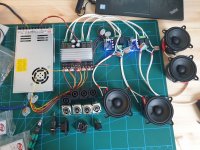
I fancied trying Class-D for my main system so last year I bought a 3E TPA3251 4x100w board and I have finally got the time and parts to do it. I also wanted to make this chassis futureproof so I can swap in other amp/PSU combos in the future, always keeping input balanced.
Components list:
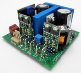
- 3E Audio TPA3251 EAUMT-0100-4-A
TPA3251-4CH-100W | 3e Audio
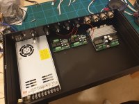
- Mean Well LRS-350-36 PSU
LRS-350-MEAN WELL Switching Power Supply Manufacturer
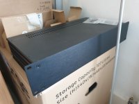
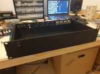
- Hifi2000 Slimline 2U Rack Chassis
HIFI 2000 Case Slimline 2U 230mm - Front 4mm Black - Audiophonics
- Speaker protection boards modified as per instructions for BTL amplifiers (x2) Power amplifier Speaker Protection Board Boot Delay DC Protect Sensitivity adjustable Stereo Amplifier Double Channel|Integrated Circuits| - AliExpress
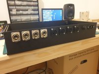
- Neutrik Speakon sockets (x4)
- Neutrik XLR Sockets (x4)
- LED mains switch
- Fuse holder
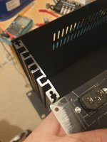
- IEC power socket
- GBPC3504 Bridge Rectifier Diode for earthing/ground
https://cpc.farnell.com/on-semiconductor/gbpc3504/bridge-rectifier-35a-400v/dp/SC07524
This should probably be straight forward, let's see")
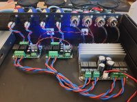
Everything is up and running as expected. The relay/protection boards are running from the auxiliary 12v power from the 3E board without issue. PSU is set to 30v as suggested by the 3E data sheet although, the heatsink does get quite warm even when idle. The 4 x 3FE25 are just my test drivers.
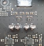
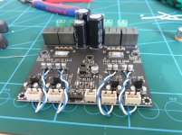
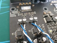
Instead of placing another component in the great audio chain I thought I would bypass the onboard op amps and go straight to the input capacitors but here is an issue! What are these extra components doing in between the coupling caps and the chip?
My plan was to remove power to the op amp, remove the zero ohm resistors and tack on to the cap can solder pad. I've checked the TPA3251 datasheet and the BTL schematic doesn't show this as a suggestion and I am not sure how to interpret what is there - an inline 100ohm resistor and capacitor going to ground.
Should I bypass this part of the circuit as well or is it important? Perhaps it is some attenuation for the op amp.
What do you guys think?
Cheers!
I fancied trying Class-D for my main system so last year I bought a 3E TPA3251 4x100w board and I have finally got the time and parts to do it. I also wanted to make this chassis futureproof so I can swap in other amp/PSU combos in the future, always keeping input balanced.
Components list:
- 3E Audio TPA3251 EAUMT-0100-4-A
TPA3251-4CH-100W | 3e Audio
- Mean Well LRS-350-36 PSU
LRS-350-MEAN WELL Switching Power Supply Manufacturer
- Hifi2000 Slimline 2U Rack Chassis
HIFI 2000 Case Slimline 2U 230mm - Front 4mm Black - Audiophonics
- Speaker protection boards modified as per instructions for BTL amplifiers (x2) Power amplifier Speaker Protection Board Boot Delay DC Protect Sensitivity adjustable Stereo Amplifier Double Channel|Integrated Circuits| - AliExpress
- Neutrik Speakon sockets (x4)
- Neutrik XLR Sockets (x4)
- LED mains switch
- Fuse holder
- IEC power socket
- GBPC3504 Bridge Rectifier Diode for earthing/ground
https://cpc.farnell.com/on-semiconductor/gbpc3504/bridge-rectifier-35a-400v/dp/SC07524
This should probably be straight forward, let's see
Everything is up and running as expected. The relay/protection boards are running from the auxiliary 12v power from the 3E board without issue. PSU is set to 30v as suggested by the 3E data sheet although, the heatsink does get quite warm even when idle. The 4 x 3FE25 are just my test drivers.
Instead of placing another component in the great audio chain I thought I would bypass the onboard op amps and go straight to the input capacitors but here is an issue! What are these extra components doing in between the coupling caps and the chip?
My plan was to remove power to the op amp, remove the zero ohm resistors and tack on to the cap can solder pad. I've checked the TPA3251 datasheet and the BTL schematic doesn't show this as a suggestion and I am not sure how to interpret what is there - an inline 100ohm resistor and capacitor going to ground.
Should I bypass this part of the circuit as well or is it important? Perhaps it is some attenuation for the op amp.
What do you guys think?
Cheers!
Attachments
Last edited:
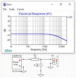
OK, so I didn't know what to search for and couldn't get the answer so my best guess is it is attenuation and a low pass filter. I did a rudimentary sim of what it might do in a crossover network and this is what I got. To me it seems to be, as I thought, post op amp correction.
Safe to remove/bypass I assume.
Safe to remove/bypass I assume.
Attachments
Puzzlement aside...
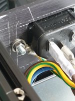
Here is the layout I will use. The connectors are as high as I could get them on the rear panel as this gives provision for different sized boards to be shoehorned in if and when I chop and change. I want to keep the heatsinks over/under the vents which also conveniently gives a very short path between input/output connectors.

In order to ensure there is an earth connection I sanded off the anodising from the side panel ends and the rear and front panel so they make a solid connection and give continuity. I just need to earth the top and bottom as well.
Which leads me to some questions that I wonder if anyone can help with, please?
According to all the well known and respected PDFs on the subject I should keep signal ground and power ground seperate. How is this possible when the power ground is one and the same with signal on this 3E board?
Hypex and Rane PDFs state that balanced shield conductors should go straight to chassis but, in this case, when ground is disconnected from the amp board it creates a buzz...?
And if the board is mounted to the chassis with brass standoffs the groud will go straight to earth anyway so the signal shield will go to chassis via this route. Bit confused on this!
Here is the layout I will use. The connectors are as high as I could get them on the rear panel as this gives provision for different sized boards to be shoehorned in if and when I chop and change. I want to keep the heatsinks over/under the vents which also conveniently gives a very short path between input/output connectors.
In order to ensure there is an earth connection I sanded off the anodising from the side panel ends and the rear and front panel so they make a solid connection and give continuity. I just need to earth the top and bottom as well.
Which leads me to some questions that I wonder if anyone can help with, please?
According to all the well known and respected PDFs on the subject I should keep signal ground and power ground seperate. How is this possible when the power ground is one and the same with signal on this 3E board?
Hypex and Rane PDFs state that balanced shield conductors should go straight to chassis but, in this case, when ground is disconnected from the amp board it creates a buzz...?
And if the board is mounted to the chassis with brass standoffs the groud will go straight to earth anyway so the signal shield will go to chassis via this route. Bit confused on this!
Attachments
Last edited:
This confused me also. According to the PDFs PIN1 should be connected to chassis as closely to the XLR socket as possible and then L&R go to the board. On the 3E Audio boards they have the audio GND connection running to the PCB signal input. I’ve wondered how this should be connected when using a balanced input....
Attachments
Yeah, all the Class-D boards I have used are the same and I have no experience (yet) with any other 'class'. In the small amount of amp projects I have done I have always gone to chassis with ground but I wanted to delve a bit deeper and do it right this time.
My thoughts were perhaps isolate the amp with nylon standoffs and route signal shield to chassis and power ground to chassis via the bridge rectifier diode unit.
The MiniDSP 10x10 in rack case is audio and power ground to chassis too - is there something I am missing or is it swimming against the tide of things done wrong?
This might (?) be true of some amplifier designs, but it's not true of the ones I'm familiar with - they all share power GND and signal GND. This is certainly the case with TPA325x and TPA311x amplifiers - you will see it in the Texas Instruments datasheets.According to all the well known and respected PDFs on the subject I should keep signal ground and power ground separate.
I think the subject of grounding is sometimes confused with the subject of earthing. All TPA325x amp boards that I know of have their GND plane exposed around the underside of their mounting holes. These amp boards are intended to be mounted via metal standoffs, making full electrical connection with the base of your metal chassis ... and of course the metal chassis should be earthed. So by design, TPA325x boards are meant to have their power/signal GND earthed. The earth wire from your incoming AC power cable can attach at any point on the chassis, but I prefer to attach this earth wire right up to one of the amp board's metal standoffs.
Now once you have earthed your signal ground at the amplifier in this way - don't earth signal ground on any other device in your signal chain! In an unbalanced signal chain, this is a recipe for ground loops. Or if you insist on doing so, at least earth that device's signal ground via a 100k resistor, which will offer sufficient resistance to any audio signal which might otherwise wish to pass that way.
That's the situation with unbalanced setups. Now to balanced:
Again, the TPA325x amp's GND should be earthed.On the 3E Audio boards they have the audio GND connection running to the PCB signal input. I’ve wondered how this should be connected when using a balanced input
Yes. In the case of a TPA325x amplifier which we have just been talking about, this is already done, via metal standoffs between amp board and chassis - so it's not necessary to connect the XLR connector's GND pin to the metal body of the XLR connector. You can do so if you wish, but it's not necessary - the GND-to-earth connection has already been done at the amplifier board.Hypex and Rane PDFs state that balanced shield conductors should go straight to chassis
If you find this confusing, draw out a diagram yourself, and you will see what I mean.
Last edited:
Thanks for the detailed answer linuxfan, this certainly clears a few things up for me. I’m reading through a thread with input from Bruno of Hypex regarding the UCD modules and he recommends connecting pin 1 of the XLR to the chassis (also removing IEC filters - something I need to do, but that’s a little off topic).
I understand with the TPA board given the audio signal is grounded to the chassis through the pcb amp module standoffs, connecting pin 1 to the chassis at the XLR is optional but really just repeats what is already done. I’m just curious as to why the advice for the ucd differs, are they a different design to the TPA or this AES best practice?
See below thread for reference.
UCD180 questions
Post #373, #379, #381, #385 and #387
Last edited:
Yes - It appears to me that the mounting holes of the UcD180HG are insulated from the GND plane, unlike the TPA325x amps, so the GND-to-earth connection needs to be made elsewhere.I’m just curious as to why the advice for the ucd differs, are they a different design to the TPA
On your UCD module, you have pins for signal positive, negative and signal ground. So we wire an incoming balanced signal with the twisted pair signal wires to the positive and neg lines on the UCD. Then we take the balanced cable shield connection straight to the chassis (not to the star connection ground point?). What is then connected to the UCD signal ground line?
This is entirely consistent with what I explained in my previous post.Connect this three wires to a XLR, whereby pin#1 of the XLR must be connected to the chassis.
Attachments
Classic "pin 1 problem". Cable shield carries error current from outside world and other equipment and there is no point to bring that current to the pcb ground. Where current flows there is voltage so "a ground" is not 0 voltage but just a reference and you don't want to modulate this reference with error currents. Cable shield is just an extension to the device chassis and the point is to protect the circuitry from outside electromagnetic fields (which induce the error current). Mandatory reading for everybody: Electromagnetoc compatibility by Henry W Ott
Of course one can bring the pin 1 to the board, I wouldn't Sometimes the "ground" currents flow a bit mysteriously and the most silent grounding scheme might not be so obvious. One can experiment with a scope and alligator clips/test leads where to ground. Remember to scrape paint between enclosure panels for proper electrical contact all around the chassis! Have fun!
Of course one can bring the pin 1 to the board, I wouldn't
Sometimes the "ground" currents flow a bit mysteriously and the most silent grounding scheme might not be so obvious. One can experiment with a scope and alligator clips/test leads where to ground. Remember to scrape paint between enclosure panels for proper electrical contact all around the chassis! Have fun!Well, that was boring. Nothing went wrong.
I got a nice email from Jason/3E Audio sayng that the resistor and capacitor after the coupling capacitor was a high frequency filter outside of audible bandwidth it it should stay put.
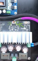
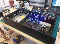
Power was removed from the op-amps, I desoldered the zero ohm resistors after and soldered cable between these and the the under side of the board so I can still use the XH connectors. All chassis panels are earthed.
The Van Damme XKE Install cable is so nice to work with - my favourite. The ground shield is already seperated and has a foil jacket. The Van Damme speaker cable used is very good too.
Once I get it installed and become accustomed I want to research tweaking the amp board.
I got a nice email from Jason/3E Audio sayng that the resistor and capacitor after the coupling capacitor was a high frequency filter outside of audible bandwidth it it should stay put.
Power was removed from the op-amps, I desoldered the zero ohm resistors after and soldered cable between these and the the under side of the board so I can still use the XH connectors. All chassis panels are earthed.
The Van Damme XKE Install cable is so nice to work with - my favourite. The ground shield is already seperated and has a foil jacket. The Van Damme speaker cable used is very good too.
Once I get it installed and become accustomed I want to research tweaking the amp board.
Attachments
Last edited:
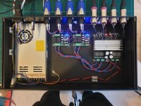
Nice build Graham. Just one thing. It is good practice and, I think, a UK regulatory requirement that the mains earth connection should be made to the chassis as close as possible to the point at which the mains cable enters the chassis.
In all my builds which use a detachable mains cable, I use one of the IEC mains socket mounting bolts as the earth point. That is very convenient and keeps the internal earth cable nice and short.
In all my builds which use a detachable mains cable, I use one of the IEC mains socket mounting bolts as the earth point. That is very convenient and keeps the internal earth cable nice and short.
Well, it needed to be connected to to the PSU earth and I wanted the unit facing forwards to keep power line and signal line apart. The top and bottom of the case isn't anodised like the sides, front and back so I wasn't confident that scratching off paint and having the top/bottom press against the sides will make a great connection. I will repeat this with the top and spur off the earth on the IEC mounting bolt. It may not be pretty but I won't have to check for continuity each time I take the top or bottom off which I plan to do for tinkering.
Yes, I discovered long ago that these aluminium project cases can have poor electrical contact between the different panels - which is potentially dangerous if, for example, a live AC wire was to make contact with the front panel of the case. It appears that the anodised surfaces are, unfortunately, good insulators.I wasn't confident that scratching off paint and having the top/bottom press against the sides will make a great connection.
My current preference is to run the incoming earth wire to the floor of the case, ideally at the same point where the amp board makes contact with the floor ...
then I carefully grind away anodised coating from the areas where screws attach the floor panel to the front, rear, and side panels. Then I replace the supplied anodised screws with raw steel screws.
Then I check electrical continuity between the panels, aiming for zero resistance.
- Home
- Amplifiers
- Class D
- 3E TPA3251 / LRS-350-36 / Hifi2000 Build