Dear all,
I was working the last couple of a weeks on a discrete PWM Class-D amplifier.
Well - basically it's not completely discrete as I still used Op-Amp IC's and integrated Power-Bridges. But still - I did the modelling of the overall control-architecture on my own.

It is a single-supply 24V BTL amplifier with differential feedback.
Here a short overview of the measurement results:
Amplifier Gain: 33.5 (26.84 Vpp out @ 800 mVpp in; 4 Ohms load)
Maximum unclipped power: 53.14 Watts @ 4 Ohms (14.58 Vrms)
Differential DC Offset: 52mV (without load), 77mV (with 4 Ohms load)
Total Harmonic Distortion (THD) @ 1 kHz
6.85% @ 1 Watt (4 Ohms load, 2.82 Vrms)
3.16% @ 10 Watts (4 Ohms load, 6.32 Vrms)
2.86% @ 25 Watts (4 Ohms load, 10.01 Vrms)
I shared all the schematics, gerber files, simulation files, measurement results on my github repository:
GitHub - YetAnotherElectronicsChannel/Discrete-PWM-Class-D
If you are interested more in detail, I did a YouTube video about this amp where I explain all the details of the design-flow YouTube
Any feedback for improvements are welcome!")
Thanks,
Markus
I was working the last couple of a weeks on a discrete PWM Class-D amplifier.
Well - basically it's not completely discrete as I still used Op-Amp IC's and integrated Power-Bridges. But still - I did the modelling of the overall control-architecture on my own.
It is a single-supply 24V BTL amplifier with differential feedback.
Here a short overview of the measurement results:
Amplifier Gain: 33.5 (26.84 Vpp out @ 800 mVpp in; 4 Ohms load)
Maximum unclipped power: 53.14 Watts @ 4 Ohms (14.58 Vrms)
Differential DC Offset: 52mV (without load), 77mV (with 4 Ohms load)
Total Harmonic Distortion (THD) @ 1 kHz
6.85% @ 1 Watt (4 Ohms load, 2.82 Vrms)
3.16% @ 10 Watts (4 Ohms load, 6.32 Vrms)
2.86% @ 25 Watts (4 Ohms load, 10.01 Vrms)
I shared all the schematics, gerber files, simulation files, measurement results on my github repository:
GitHub - YetAnotherElectronicsChannel/Discrete-PWM-Class-D
If you are interested more in detail, I did a YouTube video about this amp where I explain all the details of the design-flow YouTube
Any feedback for improvements are welcome!
Thanks,
Markus
Yes I know - I was also a little bit disappointed about that.
However - with a real speaker connected - I cannot figure out any hearable distortion even at low music levels. I compared it with my harman/kardon HK3480 receiver and personally I would not figure out which amp is who in a blind test I guess.
The only thing is that my amp is producing a little bit of noise you can hear out of the tweeter if you go with your ears up to 10cm near it.
You can also check out the speaker test in the video: YouTube
But I would really like to know how I could improve this design. Therefore I'm here
Cute. Unfortunately it would appear that the LTC6992 is going to be the main limitation on your achievable distortion figures. The datasheet...
https://www.analog.com/media/en/tec...ata-sheets/LTC6992-1-6992-2-6992-3-6992-4.pdf
Indicates that it has an internal error loop involved in generation of the PWM signal and the settling time of 8*Fmaster suggests the bandwidth of that loop is basically 1/8th of the base frequency. In your 500KHz case that would be 62.5KHz.
The above figure is not unreasonable. Pre-filter feedback involves converting the bridge switching node voltages to a triangle wave with a differential integrator prior to comparison with the reference triangle wave in the PWM modulator. The amplitude of that triangle wave at 50% duty cycle is constrained by slope matching requirements to be half of the amplitude of the reference triangle wave. If you run through the sums then that sets the ultimate loop crossover frequency at Fs/2PI where Fs is your switching frequency. Fs/6.28 is kind of close to Fs/8 give or take manufacturing variances.
However because you are forced to close your loop around the internal loop of the LTC6992 you have to do so with a loop bandwidth below 62.5KHz. How far below that is one question but as a basic design strategy it would be reasonable to proceed on the basis of slope matching using the 1V control range of the MOD input as your starting point.
Basically if you select your integrating capacitors to produce a half volt amplitude triangle wave at the MOD input your external loop would be expected to cross over at 80KHz, 500K/2PI. You can't have that so you have to increase the value of those capacitors.
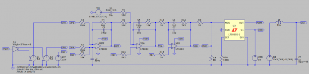
How much? Basically until the thing stops fuzzing at the extremes of modulation. The picture and .asc file is a suggestion as to how to implement the loop. C2 and C3 are the main integrating capacitors. There are two voltage error amplifiers.
If you ignore VEB then VEA gives you a first order response from DC. C4 is set the same as C2/C3 with R7 being that same as R4/R5 so the sections match and overlay. VEB adds another pole zero, C5/R12, set to be less than half the overall loop crossover. If you run the analysis with zero volts in, 50% duty cycle, the amplitude of the triangle wave at the MOD input is 300mV peak to peak. 500mV peak to peak would be 80KHz so the estimated crossover is 3/5ths this or 48KHz.
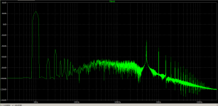
The plot shows the FFT of a close to clipping 1KHz sine wave with the indicated THD being about 0.03%. This is by and large a result of the inclusion of two Voltage Error Amplifiers to get as much loop gain as possible. In real life it will probably fall over.
There is a fundamental issue with the method used internally to the LTC6992 to achieve its PWM function. I won't go further than to say it does not like the ripple voltage that gets applied to its input as a result of this particular application. Unfortunately your THD figure will not improve if you reduce that amplitude by increasing the integrating capacitor values because you sacrifice loop gain in doing so.
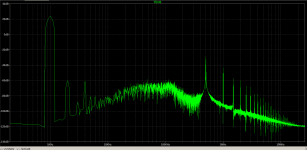
However you can improve matters by increasing the values of C6 and C7. Those were initially in place to tame high frequency instability in the LT1083 amplifiers. Setting them to 68pF introduces two extra poles at about 200KHz attenuating the ripple at the MOD input. The second FFT shows the result with the indicated THD falling to about 0.008%
...
https://www.analog.com/media/en/tec...ata-sheets/LTC6992-1-6992-2-6992-3-6992-4.pdf
Indicates that it has an internal error loop involved in generation of the PWM signal and the settling time of 8*Fmaster suggests the bandwidth of that loop is basically 1/8th of the base frequency. In your 500KHz case that would be 62.5KHz.
The above figure is not unreasonable. Pre-filter feedback involves converting the bridge switching node voltages to a triangle wave with a differential integrator prior to comparison with the reference triangle wave in the PWM modulator. The amplitude of that triangle wave at 50% duty cycle is constrained by slope matching requirements to be half of the amplitude of the reference triangle wave. If you run through the sums then that sets the ultimate loop crossover frequency at Fs/2PI where Fs is your switching frequency. Fs/6.28 is kind of close to Fs/8 give or take manufacturing variances.
However because you are forced to close your loop around the internal loop of the LTC6992 you have to do so with a loop bandwidth below 62.5KHz. How far below that is one question but as a basic design strategy it would be reasonable to proceed on the basis of slope matching using the 1V control range of the MOD input as your starting point.
Basically if you select your integrating capacitors to produce a half volt amplitude triangle wave at the MOD input your external loop would be expected to cross over at 80KHz, 500K/2PI. You can't have that so you have to increase the value of those capacitors.
How much? Basically until the thing stops fuzzing at the extremes of modulation. The picture and .asc file is a suggestion as to how to implement the loop. C2 and C3 are the main integrating capacitors. There are two voltage error amplifiers.
If you ignore VEB then VEA gives you a first order response from DC. C4 is set the same as C2/C3 with R7 being that same as R4/R5 so the sections match and overlay. VEB adds another pole zero, C5/R12, set to be less than half the overall loop crossover. If you run the analysis with zero volts in, 50% duty cycle, the amplitude of the triangle wave at the MOD input is 300mV peak to peak. 500mV peak to peak would be 80KHz so the estimated crossover is 3/5ths this or 48KHz.
The plot shows the FFT of a close to clipping 1KHz sine wave with the indicated THD being about 0.03%. This is by and large a result of the inclusion of two Voltage Error Amplifiers to get as much loop gain as possible. In real life it will probably fall over.
There is a fundamental issue with the method used internally to the LTC6992 to achieve its PWM function. I won't go further than to say it does not like the ripple voltage that gets applied to its input as a result of this particular application. Unfortunately your THD figure will not improve if you reduce that amplitude by increasing the integrating capacitor values because you sacrifice loop gain in doing so.
However you can improve matters by increasing the values of C6 and C7. Those were initially in place to tame high frequency instability in the LT1083 amplifiers. Setting them to 68pF introduces two extra poles at about 200KHz attenuating the ripple at the MOD input. The second FFT shows the result with the indicated THD falling to about 0.008%
...
Attachments
Last edited:
- Status
- This old topic is closed. If you want to reopen this topic, contact a moderator using the "Report Post" button.