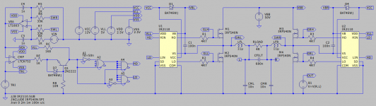
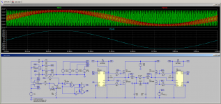
Hi I am new here and have a university project to make a diy class D audio amp and the simulation deadline is very soon. I can't figure out why the design does not like having a negative voltage at the bottom n-mos, I thought it should pull the load voltage down. Can anyone see some stupid and obvious mistakes?
View attachment Screenshot 2019-11-12 at 15.31.31.pdf
View attachment fulldrivertester.asc
View attachment Screenshot 2019-11-12 at 15.31.31.pdf
View attachment fulldrivertester.asc
You've pulled the gates to the sources with resistors - you don't do that with a gate driver chip, the chip wants a purely capacitive load for the top device gate so its bootstrapping can work. C2 is _horrendously_ large. The bootstrap cap should be about 10 to 20 times the gate capacitance normally. I think you were trying to compensate for the erroneous gate resistor.
Go study the IR2110 datasheet carefully for recommended circuits. You would be much better off using a gate driver that had programmable deadtime since you must prevent shoot-through, but you want to minimize deadtime too in class D.
The IR2110 has no shoot-through prevention at all, but you are giving it signals that will cause shoot-through. The MOSFETs explode if you do this. The simulator cannot tell you this except by the massive current spikes if you monitor the device currents.
Last edited:
10/10 for admitting to panic mode.
You should learn to drive the software to at least be able to draw pretty circuit diagrams.
I assume you know scientific notation.
What the others, who might now tumble in and slap me about, said plus...
Prior to ripping this off you might want to think about what I think I might have been thinking about. I am not knowingly right and you will look a bit silly if you cannot convincingly argue my case to your tutor.
You may wish to link to this thread in your thesis.
E&OE
...
Attachments
10/10 for admitting to panic mode.
You should learn to drive the software to at least be able to draw pretty circuit diagrams.
I assume you know scientific notation.
What the others, who might now tumble in and slap me about, said plus...
Prior to ripping this off you might want to think about what I think I might have been thinking about. I am not knowingly right and you will look a bit silly if you cannot convincingly argue my case to your tutor.
You may wish to link to this thread in your thesis.
E&OE
...
Thank you so much for this it really helped understand where I was going wrong. I was wondering the need for Q1? Is it a buffer of some sort?
its a long way starting from scratch,
it takes years of learning trial and fail for good design
DIY have working project, add what you need or remove what you dont need and finish university project
BE aware Class D have many big holes and you will go 100 % first times go in
study class D rules and design and select carefully componets, wrong mosfets give you a big nightmare
Thank you so much for this it really helped understand where I was going wrong. I was wondering the need for Q1? Is it a buffer of some sort?
Level shift from the comparator, +2.5V/-2.5V, to the dead time logic and VLL, VDD, of the IR2110, +5V,0V.
Oh... A copy of the LTC6752 data sheet is included in the zip file. I'm not certain how the LTSpice model implements the actual device but VCC to VEE is 5V max and VDD to VEE is 3.15V max. You would tie VDD to ground in the circuit as drawn to avoid hurting it.
Last edited:
The gate resistors should be nearer 10r than 100r
You need a diode anode to gate and cathode to other side of gate resistor to give some dead time.
Faster switch off than switch on is not the same as deadtime. Its also going to increase distortion, crisp switching on both edges will minimize jitter. That means accurately generated deadtime should be used, such as a high-low gate driver of the right sort can provide. Switch off one MOSFET, delay by deadtime, switch on the other. The deadtime needs to allow for the slowest total switch-off time of the first device less the turn-on delay of the second device.
Too much deadtime will work but reduces performance as the body-diodes get in on the act and they aren't linear in behaviour and have lots of charge-storage (parallel schottky diodes can be added to improve this aspect).
- Status
- This old topic is closed. If you want to reopen this topic, contact a moderator using the "Report Post" button.
- Home
- Amplifiers
- Class D
- Help with class D university project