want use GaN TO247 for high power class D to replacing mosfets
not good news,
but Transphorm GaN Power FET Portfolio - Transphorm
offer 650V TO247 GaN for up to 3,5 KW
In this case, how is it possibile to drive TO247 GaN ?
Are you sure only sine wave drive will work with TO247 GaN ?
You can also reduce the edge rate of a square wave (I.E increase rise/fall times). One trick to do this and increase dv/dt immunity is to add gate capacitance. However this is nullifying one of the big GaN advantages which is the lower switching loss. You can hand solder GaN systems parts using hot air, they show you how to do so in their app notes. I would not bother with GaN unless using advanced packages that minimise lead inductance.
Here are some app notes I would recommend reading them:
Application Notes | GaN Systems
Also they have spice models that are quite close to reality so its worth simulating designs.
Hi NMOS,
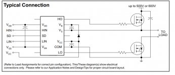
Look at LMG1210 from Texas Instruments. This is a new GaN half bridge driver with 200V rating. I am considering it for my own project.
-Len
Look at LMG1210 from Texas Instruments. This is a new GaN half bridge driver with 200V rating. I am considering it for my own project.
-Len
Im looking for 200V GaN Fet driver...psem29102i is not an option, can max 100 V
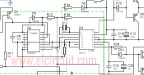
actually Im using IR2110 600V Mosfet driver to drive class D mosfets
is something similar available already for GaN ?
Hi NMOS,
Look at LMG1210 from Texas Instruments. This is a new GaN half bridge driver with 200V rating. I am considering it for my own project.
-Len
thanks,
but LMG1210 chip accept only PWM Input.
I need direct replacement GaN driver for IR2110
Im usine CD4049 / CD4070 logic - IR2110 have HIN and LIN Inputs
LMG1210 only PWM
look pic schematic
Attachments
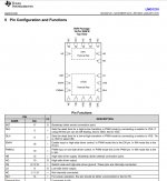
Is that so? Then why, in the feature list on the first page, does it say:
"Two control input options
– Single PWM input with adjustable deadtime
– Independent input mode"
And pins 18 and 19 have two functions (EN/HI and PWM/LI)
Hint: read page 15 of the datasheet
"Two control input options
– Single PWM input with adjustable deadtime
– Independent input mode"
And pins 18 and 19 have two functions (EN/HI and PWM/LI)
Hint: read page 15 of the datasheet
thanks,
but LMG1210 chip accept only PWM Input.
I need direct replacement GaN driver for IR2110
Im usine CD4049 / CD4070 logic - IR2110 have HIN and LIN Inputs
LMG1210 only PWM
look pic schematic
Is that so? Then why, in the feature list on the first page, does it say:
"Two control input options
– Single PWM input with adjustable deadtime
– Independent input mode"
And pins 18 and 19 have two functions (EN/HI and PWM/LI)
Hint: read page 15 of the datasheet
have check......thanks
Is GaN driver for Class D available > 200 V with independent mode ?
cant find....
I know Class D Designs working with up to +/- 160 V Half bridge
Find Electronic Components | Mouser Finland
Find Electronic Components | Mouser Finland
Find Electronic Components | Mouser Finland
You only have to search...
PS: Are there any particular / "special" characteristics a GaN driver has, as opposed to a "normal" MOSFET gate driver?
Find Electronic Components | Mouser Finland
Find Electronic Components | Mouser Finland
You only have to search...
PS: Are there any particular / "special" characteristics a GaN driver has, as opposed to a "normal" MOSFET gate driver?
[
PS: Are there any particular / "special" characteristics a GaN driver has, as opposed to a "normal" MOSFET gate driver?
Yes and no,....
GaN = class D amp will have 99 % efficiency,
Heatsink can be very very small
GaN FETs are faster resulting in superior linearity and efficiency
Dead Time 5 ns posibile
look here TO247 GaN Fets
Transphorm GaN Power FET Portfolio - Transphorm
look picture,
I want replace IR2110 with TI LMG1210 using in independent Mode
and Mosfet with GaN Fet TP65H035WSQA
Its all theoretical now, I dont know it work or not,
when lead induction is possibile, I dont know amp can work stable or not
Attachments

I was asking about the driver chips themselves, whether they were (or needed to be) anything more special than the already-existing MOSFET drivers.
sorry, its to new for me
Im collecting information for further upgrade / development witn GaN
Well, that's just it - is there something wrong with the IR(S)2110, that's somehow "not good enough" for GaN FETs? Or why do you need / want a replacement for that?
I browsed through a few of those datasheets, and they all say in the "Benefits" section on the first page, "Easy to drive with commonly-used gate drivers".
Soooooo... Yeah.
I browsed through a few of those datasheets, and they all say in the "Benefits" section on the first page, "Easy to drive with commonly-used gate drivers".
Soooooo... Yeah.
Last edited:
Well, that's just it - is there something wrong with the IR(S)2110, that's somehow "not good enough" for GaN FETs? Or why do you need / want a replacement for that?
I browsed through a few of those datasheets, and they all say in the "Benefits" section on the first page, "Easy to drive with commonly-used gate drivers".
Soooooo... Yeah.
I dont know can drive or not ?
some peple talk GaN need higher Gate voltage
but TI lmg1210 GaN driver need 4 layer to get lower loop inductance
But finally, Class D no need switching GaN in MHZ only 250 khz
theoretical it can work with IR2110
Benenfit of GaN is -30 % lower temperature, 99 % efficiency 50 % smaller PCB
and heatsink
1 Pair GaN can handle 3500 W impossible with mosfets
Last edited:
I was asking about the driver chips themselves, whether they were (or needed to be) anything more special than the already-existing MOSFET drivers.
yes they need to have minimal gate overshoot and be capable of operating at low voltages. Exceeding Vgsmax ~6V (which is very close to nominal Vgs ~4-5V) destroys the GaN FET. This is one of the reasons why TO-220 and other conventional packages are unsuitable as the lead inductance means that its very easy to exceed the Vgs rating either via the reverse transfer capacitance or by overshoot. I would recommend only using drivers that specifically mention GaN FET compatibility if you are unsure of what specifications you need.
Picked at random, page 3 of the linked datasheet seems to disagree:
https://www.transphormusa.com/en/document/650v-aec-q101-cascode-gan-fet-tp65h035wsqa/
"Recommended gate drive: (0V, 12V) with RG = 30Ω".
And specs (Rds(on), gate charge) are quoted at Vgs=10V. Sense - this isn't making any
https://www.transphormusa.com/en/document/650v-aec-q101-cascode-gan-fet-tp65h035wsqa/
"Recommended gate drive: (0V, 12V) with RG = 30Ω".
And specs (Rds(on), gate charge) are quoted at Vgs=10V. Sense - this isn't making any
That particular Transphorm device is a compound device: A silicon MOSFET whose Drain connects internally to the Source of the high-voltage GaN FET -- cascode -- thus the 'normal' drive requirements.
Sure sounds like a promising approach, but I haven't run any of 'em.
Regards,
Rick
Sure sounds like a promising approach, but I haven't run any of 'em.
Regards,
Rick
That particular Transphorm device is a compound device: A silicon MOSFET whose Drain connects internally to the Source of the high-voltage GaN FET -- cascode -- thus the 'normal' drive requirements.
Sure sounds like a promising approach, but I haven't run any of 'em.
Regards,
Rick
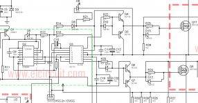
This means or not,...IR2110 can drive Transphorm GaN fets ?
Plug and play replace mosfet in Class D circuit like this with Transphorm GaN fet to get benefits ?
Attachments
Last edited:
yes they need to have minimal gate overshoot and be capable of operating at low voltages. Exceeding Vgsmax ~6V (which is very close to nominal Vgs ~4-5V) destroys the GaN FET. This is one of the reasons why TO-220 and other conventional packages are unsuitable as the lead inductance means that its very easy to exceed the Vgs rating either via the reverse transfer capacitance or by overshoot. I would recommend only using drivers that specifically mention GaN FET compatibility if you are unsure of what specifications you need.
Me thinks saying it 10 times wouldn't even help;-)
Sorry if I'm being dense, but purdy sure it's 'cause we're talkin' about 2 VERY different parts:
1- pure GaN devices, the newer ones of which are enhancement mode
2- compound HEMT devices, which are internally cascode-connected
As for the #1 types, kipman725 has first-hand experience, and has given enough specifics to discourage (hopefully) the inexperienced designer (most of the rest of us). They are completely unsuitable as direct subs for standard silicon MOSFETs. There isn't even a package in the usual sense -- you would have to invent that. And you'd get really tired of carefully replacing the blown ones, and there would be plenty.
The #2 types look like they might be useable -- the drive requirements line up closely with silicon MOSFETs because both the input Gate and the Source are exactly that. It is actually two transistors sharing one die in a cascode connection. Have a peek at:
US8084783B2 - GaN-based device cascoded with an integrated FET/Schottky diode device
- Google Patents
if you can stand the obtuse writing it takes to get a patent.
NMOS, The Transphorm cascode parts should sub successfully by most measures. But you almost certainly won't be able to hear the difference. The reason is the IR2110 and the rest of the drive circuits (shown in post 38) are dreadfully slow compared to these GaN parts. Have a quick comparison between the Dynamic Specs on page 3 of the IR2110 data sheet, and the same timings for some of the 'GaN-Approved' driver IC's on pages 17, 18 of:
https://gansystems.com/wp-content/uploads/2018/04/GN001-Design_with_GaN_EHEMT_180412.pdf
that if IRC was in an earlier post this thread. The other 43 pages are essential reading if you just can't resist the temptation to try some of these little monsters. (kipman725, was that you? -- Thanks)
mterbekke, I hope you don't have to say it 10 more times ..
Regards,
Rick
Last edited:
- Home
- Amplifiers
- Class D
- Class D with GaN FETs & IC PE29102 (GaN FET) driver