Hi Jan,
What about such a "bugger"? : 500W +/ 35V Amplifier Dual voltage PSU Audio Amp Switching Power Supply Board|Power Supplys| - AliExpress
or eventually two of those : 30v 5a switching power supply ac dc adapter 30v5a 30v dc voltage regulator 150w power supply|power ac dc|ac dc adapterdc adapter - AliExpress
Hi FF,
Your search skills are better than mine!
The one you linked to was no longer available, but I found more:
500W +/ 35V Versterker Schakelende Voeding Board Dual Voltage Psu Audio Amp Module Elektronische component|Instrument onderdelen & Accessoires| - AliExpress
Isn't it a big difference in Wattage?
500W +/-- 35V versus 2 x 150W 30V
I know it's silly, but using laptop bricks feels like cheeting, though I've used them many times when a 'proper' powersupply wasn't available yet.
Regards, Jan.
Last edited:
And another: similar in design, but with another nametag and other components (ferrite coil in one, plastic covered whatsamething in the other):
Digitale Voeding Board 500W AC200 240V 30V/35V/37V/40V/45V/50V/55V/60V/65V/70V Voor Versterker HBP500W|Oortelefoonaccessoires| - AliExpress
Prices are similar.
Regards, Jan.
Digitale Voeding Board 500W AC200 240V 30V/35V/37V/40V/45V/50V/55V/60V/65V/70V Voor Versterker HBP500W|Oortelefoonaccessoires| - AliExpress
Prices are similar.
Regards, Jan.
I own 4 Behringer B115D MP3 speakers. They use that chip in a single PCB holding the PSU & the amp. They are rated 1000W. The heatsink is the amp cage and has no fan for cooling. I use it for ambient / background music. On all of the boards the tiny undersized output inductors got cooked. They've got so hot the upper can popped out.
I have glued it with heat resistant silicone but I'm sourcing for some T106-2 cores and I will replace them.
I own other PA amps & all of them use several output drivers with heatsinks & fans. 400W RMS from such a tiny chip...
I have glued it with heat resistant silicone but I'm sourcing for some T106-2 cores and I will replace them.
I own other PA amps & all of them use several output drivers with heatsinks & fans. 400W RMS from such a tiny chip...
Last edited:
How to engage mute?
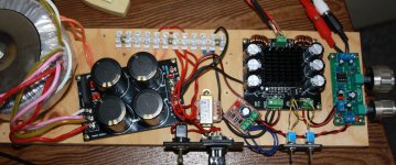
As my configuration suffers from a distinct 'thump' when I power down the amp, I added a DC protection relay circuitboard with a seperate powersupply, no more switching off noise.
I was made aware that D class amps need to see a load and are prone to damage if that is switched off by a relay.
As this board comes with a mute solder pad, I wondered if I could make use of that by muting the amp a fraction before the power is switched off, effectively avoiding the 'thump'
Unfortunately I have no idea how to engage the mute function; having read the specs on the subject doesn't help, as I don't understand what's being written...
Suggestions please.
Regards, Jan.
Answer: Yes, it's that simple.
As you can see in the picture, the two small switches on the right are conneting the two sets of solder pads, mute and standby.
I'll have to find out what the difference between 'mute' and 'standby' is, regarding powering down the amp without a 'thud' when the supply voltage sags...
Regards, Jan.
As you can see in the picture, the two small switches on the right are conneting the two sets of solder pads, mute and standby.
I'll have to find out what the difference between 'mute' and 'standby' is, regarding powering down the amp without a 'thud' when the supply voltage sags...
Regards, Jan.
Attachments
Modifications
Hi,
My plan is to make all modifications. I need help about input stage. It looks on picture 3 that C30 and C41 are removed and there is short connection on theirs place (with end of 1uF input capacitor). Is that correct?
It is hard to me to see correct how input stage is now connected to TDA chip.
Did you make cutoff of some signal ground wires on PCB?
I was tempted by this very cheap (10$) TDA8954TH board (XH-M253) promising 420W (!) mono.
XH M253 TDA8954TH Core BTL Mode HIFI Class 420W High Power Mono Digital Amplifier Board D3 003|Amplifier| - AliExpress
420W I do not need and I find it unlikely in practice but a BTL coupled amplifier, supplied with a symmetrical voltage, can easily be converted into a stereo amplifier with 25% of the power on each channel. It is in principle a matter of swapping the two input lines on one of the channels. However in practice, it may end up more demanding.
I made a schematic of the initial circuit. It is appended below.
I discovered reasons why this board should not be used “as is” without some modifications and certainly not at output levels approaching 420W.
* A serious flaw is the use of wrong values for the snubber-circuits (R9/C22/C23 and R13/C33/C34) at the two output lines of the TDA8954TH chip. The correct values are 10 Ohm and 220pF while the initial values used on the board are 10 Ohm and 220nF! The use of far too high capacitor values means that the resistors (10 Ohm) are immediately overloaded and burn to open state, with the result that the snubber-circuits are disconnected. Then, the voltage spikes at the output lines of the TDA8954TH chip are not damped at all and may harm the chip, in particular at high output levels. It is mandatory to replace the snubber-circuit components. On my board, one of the capacitors (C22) was even defect as the capacitor body was missing.
* The heatsink is far too small for high output levels. An efficient, low-noise fan will absolutely be needed. At +/-24V supply and with some 2x2W output (when changed to SE stereo configuration), my heatsink got to good 40 degrees (Celsius), with a room-temperature of 18 degrees, before I used a fan. Imagine the temperature with +/-40V supply and several hundred Watts at the output. Use a fan!
* The supply rails decoupling capacitors (6x2200uF/50V) implemented were not the “Nichicon”-type shown in the advertisement but only cheap “ChongX”-types. 6x2200uF is insufficient for high power levels and should be replaced with a reliable type in order to handle the high ripple currents.
* The output filter capacitors are of the ceramic SMD type (“0603” it seems). With +/-40V supply, I doubt that they can stand the ripple current for long. They should be replaced with film type capacitors.
* In order to reduce switching noise on the analog supply terminals of the TDA8954TH chip, the TDA8954 datasheet recommends the use of 10 Ohm resistors in-between the regular power rails and the analog supply pins of the chip. 1 Ohm resistors are used initially and should be replaced with 10 Ohm for better noise suppression.
* For use at 420W, the PCB should be of a reinforced type with particularly wide copper tracks and eventually thicker (than standard) copper foil. It is not a reinforced type but only standard and the tracks are not particularly wide. I would not take that board to 420W at the output. Modified to stereo 2x80W perhaps (+/-36V supply), but not BTL 420W.
* The output filter chokes have a value of 47uH. This leaves a cut-off frequency near 34KHz. Some will argue that it is a bit low. Worse may be if the more than 10A, for achieving 420W in 8 Ohm, may cause the chokes to saturate in part. Without knowing the specs for the cores and chokes, this remains unknown.
* The small metallic cooling-pad on top of the TDA8954TH housing is electrically connected to VSSA (pins 1 and 24). Therefore, the datasheet recommends use of an insulating sheet between this cooling-pad and the heatsink. Such is not used for the initial design. Without such a sheet, it relies on the insulation from anodizing of the heatsink.
I modified my board into stereo SE configuration by swapping the two input lines to one channel and connect the speakers between each of the output terminals and ground. I:
* replaced the initial snubber components with correct values (10 Ohm/220pF/220pF),
* used a slow-running, low-noise fan for the heatsink,
* replaced the six “ChongX” 2200uF/50V power rails capacitors with Nichicon types,
* replaced the ceramic SMD-type output filter capacitors with good film types (470nF),
* replaced the initial 1 Ohm noise reduction resistors with 10 Ohm ones,
* added two 1uF ceramic capacitors in parallel with C20 and C21 for better noise decoupling,
* replaced two signal input capacitors (C30 and C41) with 1uF film types,
* replaced the two other signal input capacitors (C40 and C26 being connected to ground after swap of input lines) with ceramic “0805”, 4.7uF,
* added two 47K resistors between each input terminal and ground,
* removed C42 and R14 that had become without purpose,
* removed the rectifier bridge and wired the board power rails directly to the power input terminals such that external power rails decoupling would be more efficient,
* stabilized the components with “thermal glue”,
* replaced the two 10uF capacitors with better quality ones as they had anyway been taken out of the PCB to give access for the modifications,
* inserted an insulating sheet between the TDA7854TH housing and the heatsink, adding a fine layer of cooling paste on both sides.
With a +/-24V supply, adding two 10000uF external decoupling capacitors, the modified stereo amplifier sounds just great. As it can be expected from an NXP top-line product. No annoying hum or other noise. I do not intend to use the amplifier above +/-36V supply (2x80W in 8 Ohm).
The board is a typical value-for-money product with good intentions but a careless implementation that necessitates some modifications and suggests further improvements. You get a functional TDA8954TH chip mounted on a reasonable PCB without any real (observed) flaws, decent output filter chokes, decent connection terminals, an acceptable heatsink (to be used with a fan), ceramic signal input capacitors (that may be used) and a mute/standby circuit that actually works.
420W output – not with my board!
Schematic: Initial implementation.
Photo 1: Board before modifications.
Photo 2: Board after modifications.
Photo 3: Rear side after modifications.
Photo 4: Final board with thermal glue for stabilization.
Photo 5: Rear side with thermal glue for stabilization.
Do you think it would be a good idea to solder wires in parallel with the power tracks to improve the current caryring capacity?
Hi,
My plan is to make all modifications. I need help about input stage. It looks on picture 3 that C30 and C41 are removed and there is short connection on theirs place (with end of 1uF input capacitor). Is that correct?
It is hard to me to see correct how input stage is now connected to TDA chip.
Did you make cutoff of some signal ground wires on PCB?
My plan is to make all modifications. I need help about input stage. It looks on picture 3 that C30 and C41 are removed and there is short connection on theirs place (with end of 1uF input capacitor). Is that correct? Yes, C30 and C41 are removed, the pads are bridged (shorted) because I use the film signal coupling-capacitors (yellow) on the rear side of the board.
It is hard to me to see correct how input stage is now connected to TDA chip.
Did you make cutoff of some signal ground wires on PCB? C40 is grounded on the side of the green connection terminals. I had to cut the previous signal line. C26 remains unchanged.
For at least one of C30 and C41, I had to cut the previous ground connection so I could use that capacitor for signal input. For one of the channels I had to swap the two inputs in order to have the same phase for both channels. Check eventual ground connection on C30 and C41 first with an Ohm-meter.
My modified TDA8954TH board still plays very well. Now stereo.
Good luck!
") .
.Hi guys,
Really good information here. Planning to do the mods myself.
The reason I was searching though is that I am getting some chirping noise from the speaker even with nothing connected. I tried with both an analogue PSU I made and with a decent DC lab power supply unit.
One thing I noticed is that at +/- 20-25VDC, the sound is more of a humming and as I increase the voltage above 30, it starts to chirp.
Any ideas?
With my first TDA8954 amplifier (a different board), I had a strangely behaving treble. Only when I realized that the snubber circuits (components values) were absolutely wrong and corrected it, I got a predictable sound.
Without knowing how a "chirping noise" sounds, it may very well relate to the snubber circuits that are likely to cause different ringing with varying supply voltage.
I am looking forward to hear about your results.
Until now I only used +/-24V supply.
Without knowing how a "chirping noise" sounds, it may very well relate to the snubber circuits that are likely to cause different ringing with varying supply voltage.
I am looking forward to hear about your results.
Until now I only used +/-24V supply.
Last edited:
 ) and now you have to strain to hear any hum at all.
 Brilliant!
Hi, I have a problem when I connect something on my input connector I have noise on output.
Nothing happen when all is open and when nothing is connected to the audio input connector.
But when I connect a cable, I have the same noise as this guy : HiLetgo TDA8954TH Mono Channel Digital Amplifier Board 420W Digital Core BTL Mode HiFi Class High Power Mono Digital Amplifier Board: Amazon.fr: Informatique
Any idea what to do?
Thanks,
A 1k resistor give more noise compare to when nothing is connected to it.
But it is less than in the video in the previous post.
Yes the modules are not modified, as delivered.
Il s'agit sans doute du 50hz du réseau edf car quand je coupe l'alimentation et qu'a ce moment là il reste un peu de jus dans les condos, je n'ai pas de ronflette. Mais malheureusement ça ne dure qu'une seconde.
- Home
- Amplifiers
- Class D
- TDA8954th btL amplifier