So I made a little progress. As I apparently lack the skills to fully understand, and even less, to design, a control loop this have been a fun exercise ")
I tried a lot of different feedback options and although some did offer lower distortion they all had other shortcomings: bad clipping, bad no-load behavior, bad start-up behavior.
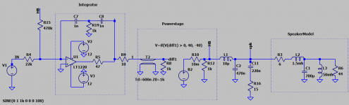
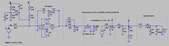
To recap, the "base-line" for my experiments are sketched in the attachment: TL072 integrator, lm311 comperator, IR2184 driver and IRF640N mosfets. Very, very basic stuff.
20Vpp over 8Ohm at approx 0.035% distortion. I would say that this is OK for my application, but the no-load behavior with a squarewave-input is pretty bad as there is no control over the output voltage.
More to come..
TroelsM
I tried a lot of different feedback options and although some did offer lower distortion they all had other shortcomings: bad clipping, bad no-load behavior, bad start-up behavior.
To recap, the "base-line" for my experiments are sketched in the attachment: TL072 integrator, lm311 comperator, IR2184 driver and IRF640N mosfets. Very, very basic stuff.
20Vpp over 8Ohm at approx 0.035% distortion. I would say that this is OK for my application, but the no-load behavior with a squarewave-input is pretty bad as there is no control over the output voltage.
More to come..
TroelsM
Attachments
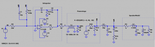
as suggested from voltwide a small cap from the output to the integrator "summing-point" makes a BIG difference with regards to controlling the output at no-load situations.
The value of the cap is shown as 22p in the attachment, but It should be changed to fit the specific circuit. 22p worked in my prototype
My understand is as follows: the output-voltage will have a 180deg phase-shift around the LC res-freq and any direct voltage feedback from that point will lead to (unwanted) oscillations. BUT the cap is not a voltage-feedback because it goes to virtual GND at the integrator summing-point. The current in the cap will be a function of the output voltage but the current is only phase-shifted by 90deg. Does that make sense? - in any case: it works.
It does not change anything else, but for the small effort, I dont see why you would not include it.
More to follow...
TroelsM
Attachments
As mentioned I tried different other feedback options in both LTSpice and prototype but none were really good.
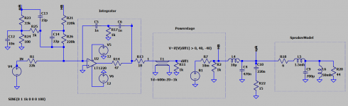
One thing looked promising and that idea is shown on the attachment. Please don't copy the values directly. They will need to be changed to fit a specific circuit.
The idea is as follows: R23/R24 is voltage-divider that is low-pass-filtered by C12. The "output" of this filter is feed to the summing-point, but this ONLY works if the cap C13 manipulates the phase around LC res.
R21 and R26 is the feedback from the halfbridge, but now C14 makes the total resistance and thus gain smaller at high frequencies.
With the "correct" values for all the feedback-components this version appears pretty stable, but it does not significantly lower distortion.
I only compared distortion at 1Khz for these test.
So, what do you say to this odd solution?
We are still not there, so stay tuned..
TroelsM
Attachments
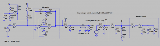
And so, the last update for today. I'm not totally sure how this idea came to me, but its something about manipulating the phase through in the loop to make it stable.
In the attachment R31, R42 forms a voltage-divider that halves the signal between the integrator and the comperator. As the LM311 only detect polarity the size of the signal should not make a difference right? -but C23 manipulates the phase and that makes a lot of difference.
The prototype can now run without C20 and still be pretty stable. And when all values are trimmed correctly I get distortion-numbers close to 0.0075% at 20Vpp/8Ohm. Squarewave-overshoot with no load is around 75% and very well controlled.
The components I trim to lower distortion is R33, R36 and R40.
R36 is the loop-gain before we apply post-filter-feedback. So more gain should result in lower distortion, but at some point it will become unstable.
R40 have some influence, but not much, so for now I'l leave it around 1K.
R33 changes more than one parameter and I'm not sure which parameter is making the difference right now. Too high and the distortion rises, too low and the feedback becomes unstable. The sweetspot do not appear to be super-narrow, so for now, I'm not worried that its border-line-stable.
More tests, to be done, but I'm pleased so far. Still need to test start-up and shut-down behavior.
For such basic components and a hack like me, I'm surprised to get below 0.01% distortion
Please feel free to comment and analyse my idea.
Kind regards TroelsM
Attachments
Last, last, one for today
There a lot of parameters to trim, -and I´m not (at all) sure about the dependencies from one to the other. This is the best I could do tonight.
Remember that the Ir2184 have a very large deadtime and a in-out delay around 800nS so that will limit performance.
Start-up and shutdown appear to be stable and controlled.
Clipping is acceptable. Switch-freq around 300Khz.
Comments?
Kind regards TroelsM
Attachments
Any inputs? - I could really use the feedback from all of you with more experience.
My first impression is that linear(ized) theory says that you are better off with all your feedback after the filter.
You just need to control the feedback loop gain correctly and the stability will be equivalent to mixed pre and post feedback but the distortion will be lower.
I just read that this is also Bruno Putzeys' position, which reassures that it's fairly reasonable.
This assumes you can "control the feedback loop gain correctly".
Until you have a linearized model to study the Return Ratio you are in the dark.
So I would make that a priority, I have started to work on it.
Linear theory breaks down once the amp clips or saturates, it may be that a two loop solution handles this more easily, that would be the only reason I can see to use it.
But I would work on this only after I had the linear case clear.
Best wishes
David
I found that your circuit is similar to that proposed by Mueta, a European brand.
They have an AES paper on it that I haven't fully studied yet.
Last edited:
Hi Dave.
Yes, FB should be good and indeed I'm getting a little less distortion with the PFFB. So far, so good. I have been poking the prototype with a stick trying to "upset" the loop and see how close we are to instability. So far it appears to be rock solid.
I have tried to:
The simple LT-spice model agrees on most of my findings, so we are not totally in the dark, but I agree that a model for gain-phase analysis would be good.
Could you link to the paper you refer to? Does that solution also include the R-R-C -stage between the integrator and the comperator? - in my test, this "filter" is essential to remain stable.
Kind regards TroelsM
Yes, FB should be good and indeed I'm getting a little less distortion with the PFFB. So far, so good. I have been poking the prototype with a stick trying to "upset" the loop and see how close we are to instability. So far it appears to be rock solid.
I have tried to:
- remove load with input signal
- squarewave with no load and inductive load
- small alterations to component-values to simulate aging and temperature-swing
The simple LT-spice model agrees on most of my findings, so we are not totally in the dark, but I agree that a model for gain-phase analysis would be good.
Could you link to the paper you refer to? Does that solution also include the R-R-C -stage between the integrator and the comperator? - in my test, this "filter" is essential to remain stable.
Kind regards TroelsM
Could you link to the paper you refer to? Does that solution also include the R-R-C...
Sure. http://www.mueta.com/MuetaAES112th5503AsyncSwitchHighEndAmp.pdf
I haven't understood it fully yet, it's not quite the way I think.
I prefer to see the linearized feedback behavior separated from the details of how the PWM is created.
Not sure if this is just a different way to look at the problem or if there is a real difference.
I suspect the details of the PWM are absorbed into the linearization.
I need to read Christophe Basso's books on SMPS to make it clearer.
My view is that your experiments simply show the results as you shape the Return Ratio of the feedback loop.
The test data all looks consistent with that view-
- post filter feedback corrects better for no load
- differentiated feedback compensates for one of the poles in the filter
Best wishes
David
Last edited:
If anyone is interested I have attached the schematic of the current version of my prototype. The feedback becomes a little xtra complicated because the only SMD caps i have is 50V types, so some of them are in series.
IC3A is a balanced input/buffer
IC3B is the integrator
IC1A is a temperature-monitor. D14 is the sensor ans is placed in contact with Q1
IC1B should trigger if the output voltage (HF) goes too high. This would indicate that the output was oscillating uncontrolled
IC3C and IC3D monitors the integrator-output. If the voltage goes too high it means that the feedback is not working ( most likely because the output clips)
T1 and T2 monitor suppl-voltage and turns IR2184 of if the voltage goes below+/-25V or above +/-55V.
The output-stage around IR2184 is very conventional. T5 and T6 are maybe not needed. The values for gate-drive are not optimzed, but it appears to work fine. Outputs are not IRF540, - but IRF640N in the present version.
As always: Please feel free to comment.
Kind regards TroelsM
Attachments
If anyone is interested I have attached the schematic of the current version of my prototype. The feedback becomes a little xtra complicated because the only SMD caps i have is 50V types, so some of them are in series.
IC3A is a balanced input/buffer
IC3B is the integrator
IC1A is a temperature-monitor. D14 is the sensor ans is placed in contact with Q1
IC1B should trigger if the output voltage (HF) goes too high. This would indicate that the output was oscillating uncontrolled
IC3C and IC3D monitors the integrator-output. If the voltage goes too high it means that the feedback is not working ( most likely because the output clips)
T1 and T2 monitor suppl-voltage and turns IR2184 of if the voltage goes below+/-25V or above +/-55V.
The output-stage around IR2184 is very conventional. T5 and T6 are maybe not needed. The values for gate-drive are not optimzed, but it appears to work fine. Outputs are not IRF540, - but IRF640N in the present version.
As always: Please feel free to comment.
Kind regards TroelsM
admirable effort thus far.
Supervisor features can be moved to a microcontroller.
- Clip Detector
- Current sense
- OV/UV/OT
- Modulator frequency monitor
Supervisor features can be moved to a microcontroller.
- Clip Detector
- Current sense
- OV/UV/OT
- Modulator frequency monitor
Yes, you got a point. I spend around 6 hours assembling the latest prototype-version. I plan to build 4-6 modules for an active speaker system, so at some point time becomes an issue, - even for an diy-project
.Hopefully that FW could be really simple ( arduino-platform) and could be re-used on all modules.
I fear that the savings in component-count would be to small to make it worth while. - but I'll definitely think long and hard about it.
TroelsM
building firmware and debugging takes its time as well. about 3-fold than expected.
so you will not save any time with a micro on board. but when it works this is very flexible.
i added the attiny 25 to my class-d modules and on the long run it was worth the effort.
with attiny25 i implemented some nice features specially for battery driven systems:
-power-up/down anti-pop logic
-undervoltage auto-shutdown taylored for my accus
-deadman logic shutting down after 15min input signal pause
Last edited:
building firmware and debugging takes its time as well. about 3-fold than expected.
so you will not save any time with a micro on board.
Obviously your comment is geared to non-pro diy design.
Its not about saving time its about building a robust system. anything worth doing will take time the benefits are obviously rewarding.
Shifting supervisor features are actually very simple, only the un-seasoned will find it challenging. Setup a few ADC's, TIMERS and IO's its a week's worth of work.
Obviously effort like this expects careful planing, and a messy unplanned approach will yield unsuccessful results.
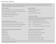
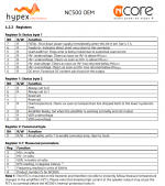
Read the NCORE and Danleysoundlabs specs for a guideline on how to do it. see attachment.
Attachments
Last edited:
Obviously your comment is geared to non-pro diy design.
Indeed that was the question to be answered. Noting more, nothing less. Thank you for your recommendations but you might have read in my last posting that I have found my solution.
- Status
- This old topic is closed. If you want to reopen this topic, contact a moderator using the "Report Post" button.
- Home
- Amplifiers
- Class D
- Class D feedback and stability