Hi all,
I have a Sanwu TDA7492 and I have no issues with it whatsoever, no pop sound or hiss, and I am perfectly happy with it. So obviously I couldn't leave it at that.
I have read that it has ready balanced input, so I was just wondering if this is true and if so, can someone point out where to solder for me?
Many, many thanks in advance and greetings from Perth, Australia.
Perth is told to be a very interesting but slightly overlooked city.
Look at figure 28 of the datasheet:
https://www.st.com/content/ccc/reso...df/jcr:content/translations/en.CD00205863.pdf
The capacitors C1, C2, C11 and C12 show the four inputs (two balanced channels). In figure 28 they expect non-balanced inputs so they just connect two inputs (C2, C12) to ground with J8 and J9. Remove that grounding through J8 and J9 and you have balanced inputs.
Last edited:
Yes, Perth is awesome, I left Europe in 2011 and never looked back.
I have the red one mentioned but it is v 2.1 (which I can't find a high res pic and my camera is crap ). I am struggling in locating J8 and J9 on my board. If i can get a high res picture, would you be kind enough to show me on the picture? Also do you know if I will still be able to use the aux input as normal?
Merci beaucoup!
This is the best I could do so far, but I will borrow a better camera and load one tomorrow. Thanks again
G'day,
The photo will probably do. The jumpers J8 and J9 are shown in that circuit diagram as example on how you can use the TDA7492 with a balanced input or with a non-balanced input. On your circuit board there are most likely no such jumpers because the designers for a start chose for an input configuration that matches the output from the Bluetooth module.
Said in other words, the input for an amplifier has to match the output from the source feeding the input. If the input source (in your case the Bluetooth module) has a non-balanced output, it is pointless to configure the amplifier used with the Bluetooth module for balanced input. You can insert a non-balanced -> balanced signal converter but unless the Bluetooth module has a very high quality, it is not worth the extra costs - you won't notice the dfference. Craftsman-wise it will be difficult to cut into the tiny connections on the board.
Therefore, for this board, accept it has been designed for the Bluetooth non-balanced output signal and even works well like that. If you want to play around with balanced inputs, buy another cheap amplifier board (TPA3118/TPA3116, TDA7492, TDA8932) without Bluetooth and make sure you actually have a source with a balanced output (only on more expensive equipment).
I know, being so pleased with the TDA7492 board make you worry if you actually fulfill your responsibility as a consumer. But, if you buy one more amplifier for input experiments you are still on the good track as a modern consumer and we will not hand-in your name as one who does not fully support consumerism.
")
Toodle-oo
Last edited:
Perth is indeed awesome. I just could not imagine the public barbecue stations in UK - they wouldn't last a day before someone weighed them in for scrap.
Daughter is at Curtin University & I have visited twice. Strangely, she wants to come home when she has finished her studies.
Particularly enjoyed the historic pumping station at Manduring Wier.
All the steam plant originally shipped from UK including economiser from local company Green's of Wakefield (still going).
@ FauxFrench
G'day mate! Thanks a lot for your help . The reason I asked the question is as I am using it as an amp for my Audio Interface as I don't want to invest in expensive monitors, which has balanced output. The manual states that it is OK to use unbalanced, but I would rather not. The other option is to build an Unbalanced to Balanced convertor of some kind, which is what I will be googling today. With Regards to the ones you recommended, which one should I go for? And by that I mean which one would be easiest to mod? Thanks Again.
@ Russc Yes, the public barbecuing is a fantastic idea and I cant believe that it is free. Your daughter will enjoy UK, but she will probably go back to Perth. Didn't know about the plants.
All the best
G'day mate! Thanks a lot for your help . The reason I asked the question is as I am using it as an amp for my Audio Interface as I don't want to invest in expensive monitors, which has balanced output. The manual states that it is OK to use unbalanced, but I would rather not. The other option is to build an Unbalanced to Balanced convertor of some kind, which is what I will be googling today. With Regards to the ones you recommended, which one should I go for? And by that I mean which one would be easiest to mod? Thanks Again.
@ Russc Yes, the public barbecuing is a fantastic idea and I cant believe that it is free. Your daughter will enjoy UK, but she will probably go back to Perth
. Didn't know about the plants.All the best
G'day,
I managed to find a couple of headphone amplifiers with balanced input and then this one:
DC12V BTL 50W Amp Board TPA3118 Mono Digital Amplifier Module Difference balanced Input or single ended input Mute Available-in Integrated Circuits from Electronic Components & Supplies on Aliexpress.com | Alibaba Group
It is only mono so you may need two.
tpa3116 mono board with balanced input: DC 12V-24V TPA3116 Mono Channel Power Audio Amplifier Board BTL Out 100W | eBay
Used it to power a passive car sub together with DC 9-32V Single Power Low Pass Filter Bass Subwoofer Pre-AMP Amplifier Board 667621528599 | eBay
Don't know about the +4db but it should do +3db compared to unbalanced input as you connect the minus input to ground.
Used it to power a passive car sub together with DC 9-32V Single Power Low Pass Filter Bass Subwoofer Pre-AMP Amplifier Board 667621528599 | eBay
Don't know about the +4db but it should do +3db compared to unbalanced input as you connect the minus input to ground.
I'm not technically qualified, but since no one else has offered an answer I will jump in. I believe the international studio level of +4 dBu is 1.228 V RMS, and 3.47 V p-p.Will the balanced input on these type of amps support the +4dbu?
The TPA3118 datasheet quotes a maximum input voltage of 6.3 volts, so you're fine.
But when using a balanced differential source, there are a couple of things to consider;
i) attenuation.
Balanced attenuation is more critical than unbalanced attenuation. The cheapest passive balanced preamp I can find is AU$45 -
Fully Balanced Passive Preamp pre amplifier XLR/RCA ALPS Potentiometer audio volume control FV2-in Amplifier from Consumer Electronics on Aliexpress.com | Alibaba Group
Otherwise you will need to adjust volume in software - that could be inconvenient.
ii) input gain.
The TPA3116/3118 chips have configurable input gain, from 20dB to 36dB, set by resistors connected to pins 7 and 8. Testing on this forum has revealed that the lower settings are necessary to avoid hiss. Since your source has a relatively high gain to start with, this setting will be even more important - you really need the input gain to be the minimum of 20dB.
If you buy that red TPA3118 board, I suggest you tell us the values (or at least the markings) of R2 and R3, then we can determine the input gain, and fix if necessary.
Hi all, and thanks for your replies. In the end I ended up buying this one:
XCSOURCE Tda7492 Amplifier Board 2X50W Class D Digital Power + Cooler Amp Board: Amazon.com.au: Electronics
The reason I went for this one was that the others from ebayl and Ali express were going to take months to arrive (thank you Australia Post) Just to clarify, the reason why I wanted balanced inputs is that my audio interface has balanced outputs. I have read that the above one, has balanced inputs but they are just grounded. I will post here when it arrives and see how I go and probably ask more questions. Once again thank you!
Yes, on the official STMicro evaluation board all that's needed for differential input is to remove jumper 8 and jumper 9 -I have read that the above one, has balanced inputs but they are just grounded.
STEVAL-CCA027V1 - 50 W+50 W dual BTL class-D audio amplifier demonstration board based on TDA7492 - STMicroelectronics
But for your Amazon board I think you will need a magnifying glass to first locate, then carefully break the traces from IN-N-A and IN-N-B to GND with a small sharp blade.
My comments regarding balanced attenuation remain.
My comments regarding balanced attenuation remain.[/QUOTE]
Thanks for responding mate. My audio interface has a potentiometer to control the volume going out so it should control the volume going in to it, right? The amp is due to arrive between 19th and end of the month, so once i get it, i will post and advise the progress (or the lack off)?
Thanks again, i really appreciate your help.
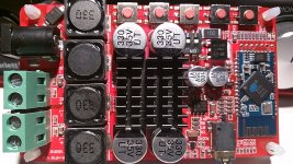
Hi again,
I got the board today and removed the heat sink to see what it needs (pic "mine"). I also found, what i think an identical modified one (pic "modified) online by someone stating that these are the mods that are needed for balanced input. From what i can see they removed capacitor C5 and C6 and also the C34, C48, C49, C8 AND C51.
I have a couple of questions that i am hoping you can help me with:
* Do i need to reconnect the capacitors C5 and C6 after the mod?
* Where would my L- and R- connect to (I am guessing that the L+, R+, and Ground will connect to the usual place)
* Will i need any resistors? and,
* Am i missing something?
Once again thanks in advance
That modified board has extensive component removal, possibly to be connected to some off-board components, but I believe they went too far - C34 and C8 should not be removed.
Here's the situation with your board:
C45 and C9 are effectively DC blocking caps for the differential -ve inputs, and since the board is configured for unbalanced input, these caps presently go to GND.
Normally I would suggest you break this connection to GND, then the newly exposed ends of these caps would become the L- and R- inputs ...
but these caps are clearly different to the large orange DC blocking caps on the +ve inputs, and ideally they should be matched - so I suggest you replace all of them ie. buy 4x blocking caps. Others here may chime in with suggestions on good/better/best caps, but the Nichicon Muse Green seems to be a go-to product for this purpose -
UES1HR47MDM Nichicon | Capacitors | DigiKey
By the way, your board has 1uF caps, but the datasheet specifies .47uf
For the +ve inputs remove the 2x orange caps, and replace with the new Nichicons.
For the -ve inputs;
- remove C45, then connect a Nichicon to the exposed pad (or for stability, the metal edge of C49) and from from the other leg of the cap to your L- source.
- remove C9, then connect a Nichicon to the exposed pad (or for stability, the metal edge of C51) and from from the other leg of the cap to your R- source.
And finally, I see a 22ohm resistor in series with the +ve inputs. I think these are unnecessary, so you can bypass them by putting a small solder blob over them. But if you decide to keep them, you should add a 22ohm resistor in series with the -ve inputs, so your +ve and -ve inputs are matched.
Thanks for the explanation mate! Can I just clarify that i understood correctly. I should remove the C9 and connect one leg of the cap (Nichicon) to the board (side closer to microchip)and the other one to the R- input (do the same for C45). That way i don't need to cut the ground. Or alternatively cut the ground, replace the capacitor and connect input on side further from chip. From memory caps less than 1uF don't have polarity so i wont need to worry about it, right?
Correct.I should remove the C9 and connect one leg of the cap (Nichicon) to the board (side closer to microchip)and the other one to the R- input (do the same for C45).
Now that I think about it, though, I don't like the idea of the Nichicon just sitting up above the board, supported only by this tiny solder connection. It would be better to lay the Nichicon on its side, or top, somewhere at the edge of the board, stuck down with a small blob of silicon. Then bend one leg of the Nichicon across to the connection point.
- Status
- This old topic is closed. If you want to reopen this topic, contact a moderator using the "Report Post" button.
- Home
- Amplifiers
- Class D
- Balanced Input on TDA7492