Hi All,
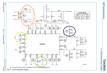
I've been intrigued by class D as of late and I'm thinking of making a couple boards up as an experiment. The NXP TDA8953/54 seem to be the most powerful monolithic ICs I can find but I'm having trouble dissecting the schematic. There are a few things that don't makes sense to me. Attached is a screen shot of the schematic with some features circled.
As an aside, is anyone seeing a difference between TDA8953 and 8954?
Thanks,
Brian
I've been intrigued by class D as of late and I'm thinking of making a couple boards up as an experiment. The NXP TDA8953/54 seem to be the most powerful monolithic ICs I can find but I'm having trouble dissecting the schematic. There are a few things that don't makes sense to me. Attached is a screen shot of the schematic with some features circled.
- Purple: What is the purpose of coupling the outputs to the supply rails? Is it to make PS noise common mode at the outputs? Would CVP1 and 2 be serving a similar purpose?
- Green: Is there a reason these caps need to be terminated to the negative supply rail? Would terminating them to ground be any different functionally? Maybe I missed this in the datasheet.
- Yellow: Since the inputs are AC coupled and there are no requirements for setting DC bias on these pins can I assume the inputs self bias? Is this common for class D chips?
- Orange: RVDDA and RVSSA seem to serve no purpose becuase they terminate back to the power supply bus (VDD and VSS). It looks like a schematic error (I checked some of theri other chips and it is the same) should these be dedicated for VDDA and VSSA?
As an aside, is anyone seeing a difference between TDA8953 and 8954?
Thanks,
Brian
Attachments
Green - You can't really change the internal design of the chip, so if those parts of the circuit are (or need to be) referenced to the negative rail... you'll probably wanna stick with that ")
Orange - Most likely / logically, the VDD / VSS on the left are the supply rails coming from your supply, and the ones on the left ("after" the series resistors) are the IC's pins (8, 11, 13, 16).
The 8954 seems to have the two diagnostic output pins (DIAG1/2); they're "not connected" on the 8953.
Orange - Most likely / logically, the VDD / VSS on the left are the supply rails coming from your supply, and the ones on the left ("after" the series resistors) are the IC's pins (8, 11, 13, 16).
The 8954 seems to have the two diagnostic output pins (DIAG1/2); they're "not connected" on the 8953.
Last edited:
Green - You can't really change the internal design of the chip, so if those parts of the circuit are (or need to be) referenced to the negative rail... you'll probably wanna stick with that
I surely will. Honestly I wouldn't even have asked if the terminations weren't through capacitors. If they are AC coupled why would it matter what the DC potentials are?
Orange - Most likely / logically, the VDD / VSS on the left are the supply rails coming from your supply, and the ones on the left ("after" the series resistors) are the IC's pins (8, 11, 13, 16).
This has to be the case. I notice now that despite the post-resistor nodes still being call VDD/VSS, the IC pins themselves are named similarly to the resistors.
The 8954 seems to have the two diagnostic output pins (DIAG1/2); they're "not connected" on the 8953.
Thanks, can't believe I missed that.
Those aren't "terminated", or "AC-coupled"; rather, the STABI pin is, as per the pin description on page 5, "decoupling of internal stabilizer for logic supply", and the PROT pin is decoupling capacitor for protection (OCP).
Had these chips been designed to be single-supply (not +/-), the internal circuitry, at least for those two blocks, would indeed be referenced to ground. Here, it's referenced to the negative-most supply rail (which, coincidentally, would be ground, in a single-supply amp).
Had these chips been designed to be single-supply (not +/-), the internal circuitry, at least for those two blocks, would indeed be referenced to ground. Here, it's referenced to the negative-most supply rail (which, coincidentally, would be ground, in a single-supply amp).
TDA8954 questions
Purple: This seems to be a "snubber" circuit that consumes spikes at the switching moment caused by the filter inductance. I have seen this snubber circuit implemented with a 10K resistor instead of 10 Ohm! Then it is without effect and the TDA8954 chip may be (voltage) stressed and malfunction (mine did).
Green: It depends on the internal design of the TDA8954. I would do what NXP recommends as the best unless you have particular reasons to deviate.
Yellow: Yep, monolithic class D amplifier chips are designed with the intent to reduce manufacturing costs. Tripath used to bother about manual adjustment of the output DC offset, nowadays it is rarely seen. The DC offset at the output should be "reasonable" if the recommended circuit, shown in the datasheet, is used.
Orange: I get your point. The 10 Ohm resistors seem just to be shorted. They may be intended as spike damping resistors and the two VDD and VSS connection points may be at different places along the same power rail.
Purple: What is the purpose of coupling the outputs to the supply rails? Is it to make PS noise common mode at the outputs? Would CVP1 and 2 be serving a similar purpose?
It's probably a stability thing for the output transistors.
Green: Is there a reason these caps need to be terminated to the negative supply rail? Would terminating them to ground be any different functionally? Maybe I missed this in the datasheet.
Not sure ... it might be a stability thing.
Yellow: Since the inputs are AC coupled and there are no requirements for setting DC bias on these pins can I assume the inputs self bias? Is this common for class D chips?
Yes. When idling the comparitor will switch at the 50% duty cycle producing 0 volts (relative to ground) on the output.
Orange: RVDDA and RVSSA seem to serve no purpose becuase they terminate back to the power supply bus (VDD and VSS). It looks like a schematic error (I checked some of theri other chips and it is the same) should these be dedicated for VDDA and VSSA?
I think it's a misnomer. Check pins 18 and 20.
The purple, snubber, can't be stability, the output devices are not amplifying, they are switched hard-on or hard off (both states of zero gain). What it does is likely damp any ringing, and routes those currents into the rails rather than ground to keep ground cleaner?
The time constant is about 5ns, which is pretty short, but then the chip's output devices are likely very fast.
The time constant is about 5ns, which is pretty short, but then the chip's output devices are likely very fast.
- Status
- This old topic is closed. If you want to reopen this topic, contact a moderator using the "Report Post" button.
- Home
- Amplifiers
- Class D
- TDA8954 Trying to Understand Reference Schematic