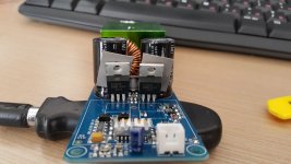
Saw this tiny 500W amp board on Ebay.
IRS2092S 500W Mono Channel Digital Amplifier Class D HIFI Power Amp Board J3K7 191466622261 | eBay
Are the figures for this general type of amp even believable, or are they a total exaggeration? Thinking of using a pair to drive a pair of 15" subs in relatively small sealed boxes with a Linkwitz transform equaliser. Not to a very high sound level but I expect the overall efficiency will be down the toilet. Also thinking of experimenting with 3 boards as a low voltage 3-phase AC source for driving a motor. Just for fiddling around, nothing practical.
So... is this kind of board worth the trouble?
Edit -> updated broken link
Last edited:
I'd suggest checking out these amps....
http://stores.ebay.com.au/sure-hifi/Audio-Amplifier-Board-/_i.html?_fsub=18214263010
I bought a 2x400W amp for driving subs. The quality is excellent
http://stores.ebay.com.au/sure-hifi/Audio-Amplifier-Board-/_i.html?_fsub=18214263010
I bought a 2x400W amp for driving subs. The quality is excellent
since the IRS2092 is a mosfet driver chip that can operate up to +-100V and with proper circuit matching to its MOSFETS can achieve 0.01% distortion figures, and the end efficiency and power handling is entirely due to the quality of the MOSFETS and inductor, the quoted 380W into 4Ω 0.1% distortion with +-65V power seems quite believable. you could even bridge them and push 760W into 8Ω. If it were me, I would probably upgrade the heatsink, if not the mosfets and the filter inductor, and the power capacitors too ... but then you might as well get the bigger version to start with...
if you're only going to be running for short periods at high levels then it might last a while, but it looks altogether too tiny to be asked to do anything demanding ... but it might be fun finding out!
if you're only going to be running for short periods at high levels then it might last a while, but it looks altogether too tiny to be asked to do anything demanding ... but it might be fun finding out!
They give the numbers themselves:
380W (± 65 power 4 ohm speaker, distortion <0.1%)
280W (± 65 power 8 ohm speaker, distortion <0.1%)
That sounds reasonable and is still a lot of power for the buck. And the output inductance looks like it can take enough power too. The majority of cheap amps lack sufficient dimensioned output coils.
@JohnnyInBris: I also bought the 2x400W amp. It sounds very good but it does not reach the stated maximum power either. To take ~20% off of the power specs seems to be much more realistic.
the quoted 380W into 4Ω 0.1% distortion with +-65V power seems quite believable. you could even bridge them and push 760W into 8Ω.
Uhm, into 2Ω - no?
Saw this tiny 500W amp board on Ebay.
IRS2092S 500W Mono Channel Digital Amplifier Module Class D HIFI Power Amp Board | eBay
Are the figures for this general type of amp even believable, or are they a total exaggeration? Thinking of using a pair to drive a pair of 15" subs in relatively small sealed boxes with a Linkwitz transform equaliser. Not to a very high sound level but I expect the overall efficiency will be down the toilet. Also thinking of experimenting with 3 boards as a low voltage 3-phase AC source for driving a motor. Just for fiddling around, nothing practical.
So... is this kind of board worth the trouble?
Class D is not a fully "open" field for mistakes, those Chinese are copying, their sources are application notes from International Rectifier and designs from engineers. The parts they use are mostly surplus, but from known brands.
In the process of developing this tiny module someone discovered that a switching regulator SO-8 IC can be used to obtain the gate drive supply rail for IRS2092, referred to -Vcc, and by the way used those 12V to power a fan, maybe even temperature switched with a transistor and NTC.
Otherwise you are going to find a copy of IRS2092 application circuit recommended by IR, maybe with some tweaks taken from others. The FETs are probably going to be surplus from IR or Fairchild, not the best in thermal efficiency, but there is a fan. Class-D modulation used is not going to be top notch (flat regardless of load), but accurate for experimental LF purposes. Output HF damper is implemented with a SMD resistor, this is not very rugged against HF use, but satisfactory for subs. Do not abuse at trebble freqs.
Overcurrent is probably going to cause shutdown, but since threshold is measured as voltage drop across FETs, higher temperature reduces threshold by as much as 2:1. Basic functions are dictated by the IC used. Description mentions DC protection, which is usually implemented with few transistors and diodes shutting down IRS2092, not going to work if a FET is shorted, for that purpose a relay or PSU shutdown is needed, like in class AB. But overcurrent works as a first defense against overload, and thermal shutdown they mention does that too, so a FET is usually shorted due to probe slip or accident in manipulation, or manufacturing defect, or maybe too fast overheat, only.
So it is a creative implementation of IRS2092 datasheet circuit. And there seem to be dozens of creative implementations like that, but the ones in the other website (sure electronics) are more expensive and maybe harder to reverse engineer.
It's not worse than the various class AB kits that have been sold for ages, like XXI century's BD139/140 and 2N3055s class AB kits. I learned class AB with stuff like that.
Last edited:
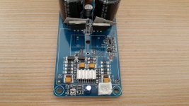
This board uses 2 MOSFET transistors IRFB31N20D, which have total gate charge between 70 and 110nC!
IRS2092S chip can operate properly with MOSFETs with less than 40nC total gate charge!
So this board can not deliver 500W...
The self noise of the board is very high - when the input is shortened.
IRS2092S chip can operate properly with MOSFETs with less than 40nC total gate charge!
So this board can not deliver 500W...
The self noise of the board is very high - when the input is shortened.
Attachments
This board uses 2 MOSFET transistors IRFB31N20D, which have total gate charge between 70 and 110nC!
IRS2092S chip can operate properly with MOSFETs with less than 40nC total gate charge!
So this board can not deliver 500W...
The self noise of the board is very high - when the input is shortened.
by my calculations with 1amp drive those fet's should rise/fall in about 50ns, so with long dead time and lower frequency it should still all be fine... though maybe with a slight increase in distortion. does that preset pot. set osc. freq?
did you stick a 'scope on it yet to see switching waveforms? what frequency is it working at?
calculations also tell me the fet's dissipate <25W heat at 11A RMS, 200kHz Fosc so maybe that tiny heatsink will manage...
have you run it at all hard to see how hot it gets?
I would guess the noise is from the buck reg. onboard, that tiny bobin inductor looks horrible... how much noise is "very high" relative to the 60V output swing?
For the price it's so tempting, but if it blows up and takes the speaker out with it then it's not so much of a bargain. Hmmm....
Maybe put fuses on the power lines? 8A on each rail should allow full power but blow if there's a fault. Those little capacitors won't be enough to blow any speaker that can take the full power of that amp...
You've got an keen eye. It's not very close, that's true but the path is quite straight. The layout could be changed but that would mean that the path wouldn't be straight anymore (or would have to switch layer two times) which would introduce a higher inductance and it would increase the distance of the mosfets to the rail capacitors too, which would introduce other drawbacks. So I'm not sure that would be a better choice. I think that has to be judged by the behaviour of the amp in actual action.
In the photos the mosfet gate resistors are a long way from the gate pins. I expect they should be right up next to the mosfets to minimise the effects of the track inductance e.g. ringing and overshoot, and the tendency of the mosfet to oscillate all by itself.
This happens mostly in linear circuits involving significant source and drain inductances, and with old MOSFET. In switching circuits drain and source inductances are the ones to minimize. Some gate inductance in switching circuits actually results in faster switching, this happens as the time constant achieved (L/R) is long enough that it allows to counteract some of the inductive voltage drop across source inductance that opposes to any switching command (faster current increase/decrease due to reduced local feedback).
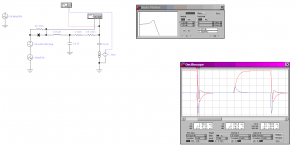
Attached picture shows a circuit I was calculating yesterday. The diode simulates a PNP buffer. The 150nH come from some folded trace length like 4 inches in 4 layer PCB. The 0.3nF come from protective zener at about Vz/3. The 4 ohm come from gate fusible resistor and trace. The 8.5r are internal FET gate resistance. The 0.6nF are gate capacitance (FET off), this is a 600V FET in SMPS, and it has to turn off into a small capacitor, fast enough to achieve low loss. The turn off gate current pulse is >.6A for 20ns (more resonance provided by real circuit since gate capacitance when ON is as high as 2nF). The FET is IPD60R450E6. Semi-resonant gate drive using PCB and zener/TVS parasitics.
This is in memory of some old geniuses fearing FETs and spreading fear to things that could actually be used for good. Take a look at the capacitance plots of a modern high voltage switching FET like the one used in this case, tailored for improvements with some gate inductance.
Attachments
Last edited:
- Home
- Amplifiers
- Class D
- Ebay amp - is 500W believable?