Altho this is no Kindergarten, we need some German here. At least my mouth does not become spelled myth.Please learn English and please try to be specific! Some of your sentences are very hard, sometimes impossible to decode.
Obviously this is false in case of ClassD (due to its definition). I don't have a clue what you wanted to say really.
Class-D is pulse width or rate modulation running on push-pull hardware. The difference between an output stage for linear Class-B and for Class-D is, just as you wrote, that Class-D needs an overflow path for Gegeninduktion, as the load is hily inductive, and at the same time the amplifier is always at full scale. Whereas Class-B needs this path only in case of malfortune as for example switching off the amplifier, while it is very busy.
You may not admit your approval of this topic, yet i expect to one day find you having silently applied it.
Last edited:
Forum rule: English posts.
So if I decode your "answer" (?) well you simply forgot to include the words "both" and "at the same time", and unneccessarily mentioned the feedback that has no relevance in that statement. Still don't know what is the relevance/context of the whole sentence.
You are offtopic in your own topic. You don't need my approval. I see you started to discover ClassD this is why I try to help you.
I want to insert some background bout general rules of operation of Class-D into this field, because all I see are chip codes, and relying on ICs is not exactly DIY. I have something to say but also miss much to know, so we can exchange ideas.
Here is a new virtual circuit:
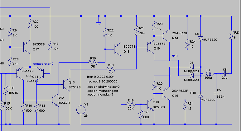
For sake of simplicity, this one is not self-oscillating and without feedback, not shown triangle generator, signal input with 3V DC bias and 6V pre-amp power supply.
Avoidance of saturation of output transistors works by power diodes D5 and D6, which lower Gegeninduktionsspannung (I think, you call that Back EMF voltage) of L1, so collector-to-emitter voltage of Q14 does not exceed zero. For you know, saturation means, that the transistor is fully on, and |Vce| is smaller than |Vbe|. Without these diodes, I would get major shoot-thru, say useless spikes of power draw.
With signal of 4KHz -20dBfullscale, there is k2 -60dBfs and a few mW of 64KHz. Complete power loss is battery-friendly, and efficiency stays in Class D manner up to full scale. It could be higher, if there were not shoot-thru at one quadrant of the signal:
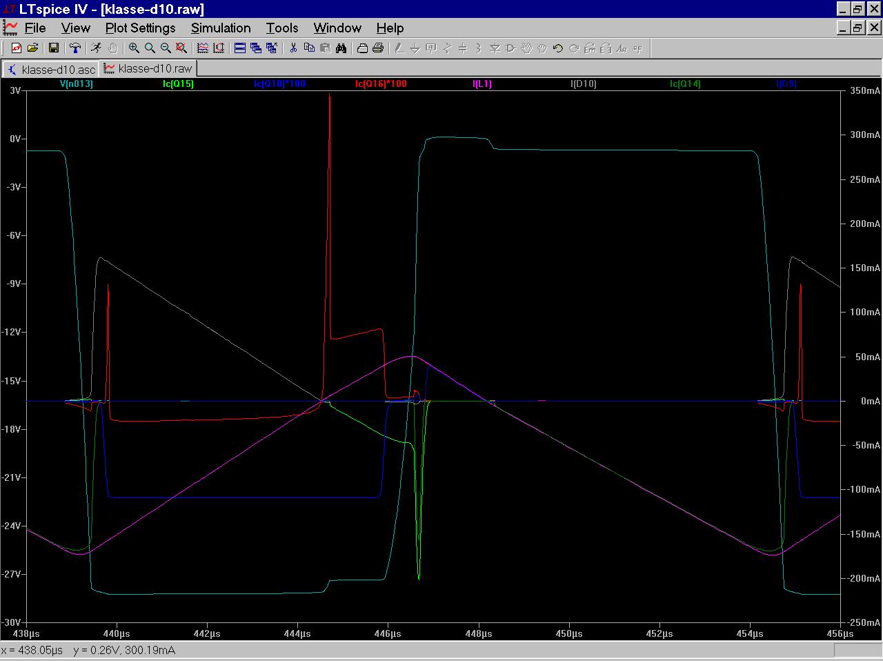
Only a fraction of a microsecond but with current as hi as signal. Anyway, see how L1 current is patched from Q14, Q15, D9 and D10 currents. Currents of Q16 and Q18 as also shown may be of less interest than of Q19, and I would be glad to get rid altogether of shoot-thru without having to add another pair of power diodes.
Switching range I cannot simulate with my 32bits machine, so I attach the .asc here and will build an amplifier and try to measure.
Here is a new virtual circuit:
For sake of simplicity, this one is not self-oscillating and without feedback, not shown triangle generator, signal input with 3V DC bias and 6V pre-amp power supply.
Avoidance of saturation of output transistors works by power diodes D5 and D6, which lower Gegeninduktionsspannung (I think, you call that Back EMF voltage) of L1, so collector-to-emitter voltage of Q14 does not exceed zero. For you know, saturation means, that the transistor is fully on, and |Vce| is smaller than |Vbe|. Without these diodes, I would get major shoot-thru, say useless spikes of power draw.
With signal of 4KHz -20dBfullscale, there is k2 -60dBfs and a few mW of 64KHz. Complete power loss is battery-friendly, and efficiency stays in Class D manner up to full scale. It could be higher, if there were not shoot-thru at one quadrant of the signal:
Only a fraction of a microsecond but with current as hi as signal. Anyway, see how L1 current is patched from Q14, Q15, D9 and D10 currents. Currents of Q16 and Q18 as also shown may be of less interest than of Q19, and I would be glad to get rid altogether of shoot-thru without having to add another pair of power diodes.
Switching range I cannot simulate with my 32bits machine, so I attach the .asc here and will build an amplifier and try to measure.
Attachments
- Status
- This old topic is closed. If you want to reopen this topic, contact a moderator using the "Report Post" button.