Update Aug 26, 2016: See post #61 on page 7 for Eagle files, BOM, and Gerbers, as well as pics of the final board.
Original post:
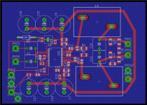
I am working on a tpa3118d2 PCB. This is literally the first PCB I've ever designed. It's not yet fully complete, but I'd like to think I'm done with the major design, and getting to the fine-tuning phase. So I was hoping to solicit some comments, critiques, tips, etc.
My main goal here was to familiarize myself with the PCB design and manufacturing process.
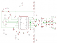
The schematic is an almost verbatim copy of DUG's DUG-1 PBTL board. DUG was nice enough to let me copy his design. It's not as fancy as the GMARSH Wiener boards, and that's not what I'm going for. I really like the DUG-1 boards, and basically want those with a few small tweaks:
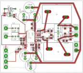
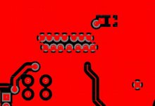
I haven't created the ground plane yet, only the signal and power lines are routed.
I know there is an error on the output side, it seems Eagle is omitting a net.
Thanks for any feedback!
Original post:
I am working on a tpa3118d2 PCB. This is literally the first PCB I've ever designed. It's not yet fully complete, but I'd like to think I'm done with the major design, and getting to the fine-tuning phase. So I was hoping to solicit some comments, critiques, tips, etc.
My main goal here was to familiarize myself with the PCB design and manufacturing process.
The schematic is an almost verbatim copy of DUG's DUG-1 PBTL board. DUG was nice enough to let me copy his design. It's not as fancy as the GMARSH Wiener boards, and that's not what I'm going for. I really like the DUG-1 boards, and basically want those with a few small tweaks:
- Use of Coilcraft VER2923 inductors to save some board space
- Room for through-hole input capacitors (actually I'll probably tweak the design a bit so you can use either SMD or leaded)
- Room for multiple OS-CON caps
- Room for leaded caps in part of the output filter
I haven't created the ground plane yet, only the signal and power lines are routed.
I know there is an error on the output side, it seems Eagle is omitting a net.
Thanks for any feedback!
Attachments
Last edited:
Only C7 and C8 are in the HF path of power decoupling, the other 4 aren't. Output stage isassymetric, wouldn't do that.
Thank you, doctormord.
Would you be willing to elaborate a bit?
Specifically, with regards to "only C7 and C8 are in the HF path of power decoupling", why aren't the others in the path? What have I done wrong or failed to do?
With regards to the asymmetric output stage: do you mean in terms of the circuit (schematic) or the PCB design? I believe the circuit should be symmetric. Though it is obvious the routing wires aren't symmetric. I can understand why the circuit should be the same, but is that also necessary for the PCB layout?
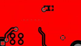
I had (at least) one known problem with the output wiring, I now believe it's fixed in the attached picture. I shuffled stuff around a bit too for a more compact and hopefully better overall layout.
Thanks again!
Attachments
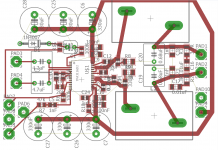
I think you should add the ground plane and see what that looks like - for me at least it saves confusion over which air wires still need to be routed.
Agreed. The real reason I didn't post the ground plane is that it turns the whole board background blue, and makes everything else even harder to read.
 I'm doing this with the free version of Eagle, so if there's a smart way to have the ground plane filled and still keep things somewhat readable, I'm all ears!
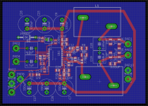
Suggest you hide layer 27 as well (top side component values) to reduce the clutter
Done! Definitely much less cluttered.
Attachments
The higher the frequency the more narrow the current will follow the path with least impedance. If you look at your latest board design and think of the current "flowing" from your input terminals to the amp pins, you'll notice that C26/27 are not in the current path - they're on a stub. So they won't help to decouple.
For the output stage, you want to have them symmetrical because of all the parasitically influences to your filter. (inductance, capacitance) As there's switching HF, unsymmetrical layout increases the chance for increased EMI, distortion, etc. Beside this, keep all high current and HF traces/areas short and tight.
Beside this, your TPA3118 is missing thermal vias under the package for heat transfer and low impedance ground connection. Actually the PVCC stubs blocks the ground route when just filled on top.
Every (power/signal) trace has n return path, even if you don't see them because all is "ground" potential.
Last edited:
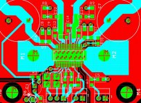
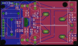
Here's the Wiener TPA breakout for reference.

I've got fat copper traces side by side bringing PVCC and ground into the TPA from above and below, to lower the inductance between the decoupling caps and TPA as much as possible.
Takes a bit of playing with the properties of polygons (rank, thermals, isolation, width, etc) to make the layout work like that, but it's good stuff to figure out.
Also, good news: the latest Pro and PBTL PCBs just came in, so I can confirm the VER2923 footprint works
Thanks everyone for the suggestions, keep 'em coming!
Is this any improvement? I tried to make the output side symmetrical. It's not a perfect mirror, as that's going to be very hard with the way those inductor leads are offset.
One thing that's not clear to me: do I need to explicitly add all the vias where a lead or pad goes to the ground plane (bottom layer)? All the air wires are gone, but I'm not sure if I sent this in now for manufacture if I would get what I expect.
I know the label says tpa3116, but this design is for the tpa3118. Saving precious close-to-IC space by giving up the heatsink and using the groundplane for heatsinking. I tossed in some vias where the tpa3118 thermal pad should be...
Thanks again!
Attachments
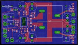
Yeah, I have a bed of nails test jig for testing boards with just the TPA3118 installed.@Gmarsh, what are these two vias beside the PVCC pins (under the IC) for?
Test-Jig?
Thoughts on this revision?
...
- I "pinched" fat traces where they ran though component pads to force current through the device
...
I take a different approach to this. I want a good connection and low impedance wherever possible.
Into an inductor the trace length is not important for inductance reasons but for resistance reasons.
Into an RC the trace length is not important for resistance reasons but for inductance reasons.
For capacitors I try to use the shortest / widest trace. (relative to what the capacitor is doing) For bypass or filter surface mount capacitors I sometimes use two or three traces to vias to ground. For the input caps this is not critical because the input impedance of the IC is very high relative to the trace impedance.
On another note.
In OrCad Layout ( and probably other programs as well) the copper pour automatically forms around vias and component pads and connections are made with what are called thermal reliefs. These allow the pad to be soldered with a minimal of heat sinking to the copper pour.
I use copper area to "override" these thermal reliefs to get a continuous connection to the vias or component pads. You need more heat for soldering a TPA3118 but that is the point...better thermal conductivity to the copper ground plane. (and lower impedance)
One example is multiple vias under the IC.
Attachments

Thanks Doug!
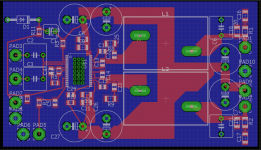
I think I'm making some progress. After some thought, I realized that this is my first ever PCB, so perfection is unlikely. And even the experts have different opinions as to what defines "perfect". So at this point I'm going for does nothing blatantly wrong.
Some changes I made:
The main thing I'm not sure of now is how to add pads on top and bottom for actual tpa3118 soldering...
Otherwise, how's this revision look?
I think I'm making some progress. After some thought, I realized that this is my first ever PCB, so perfection is unlikely. And even the experts have different opinions as to what defines "perfect". So at this point I'm going for does nothing blatantly wrong.
Some changes I made:
- Did away with one pair of PVCC electrolytics (mostly to save space)
- Output filter is now all SMD (except for "deliciously overkill" VER2923 inductors)
- Used more room on the input side to support big fancy input caps (todo: add more holes/pads for smaller or even SMD input caps ala Folsom tda7297 board)
- Used actual terminal parts instead of just generic "pad" for connections to/from other boards/PSU/speakers
- Dipped my toe in some fancier features of polygons to make fat but tidy traces
- Added a top layer ground plane ala Gmarsh Wiener board
- Offset the output inductors a bit to get a fairly symmetrical output layout
The main thing I'm not sure of now is how to add pads on top and bottom for actual tpa3118 soldering...
Otherwise, how's this revision look?
Attachments
If you go for this big/expensive inductors, stay also with MKP caps in the output filter. Of course, MLCC is mostly fine but they perform worse than MKP (MKT is okay to). I did extensive simulations on this aspect.
Running traces under an inductor is normally a "no/don't". Even if the inductor is shielded and orientated like so, some amount is HF will couple into the trace.
Are your screw holes on any grid dimension or do I need to drill four holes with a stencil?
Fill up the outputs pin connections with copper to make them more solid.
The VIAs under the chip belongs to GND so they need solid connection to this potential.
What about D1/C1/R11?
An filters for GVDD/AVDD should be as close to the chip as possible.
Last edited:
If the trace is parallel to the inductor, you'll get some coupling, but if it's perpendicular like it is here, you should be fine. Also, any induced current in that trace will be nothing compared to the current ripple in that same power trace resulting from the TPA's own switching.Running traces under an inductor is normally a "no/don't". Even if the inductor is shielded and orientated like so, some amount is HF will couple into the trace.
I run traces under inductors all the time, as long as you understand the implications of doing it and make sure it's mitigated or insignificant, it's fine.
- Status
- This old topic is closed. If you want to reopen this topic, contact a moderator using the "Report Post" button.
- Home
- Amplifiers
- Class D
- My tpa3118 board - comments/critiques?