I had a need for a 5V amplifier, and a quick search showed the easiest commonly available module is based upon the PAM8403, and cost about $0.50 per unit.
10 Pcs PAM8403 2X3W Mini Audio Class D Amplifier Board 2 5 5V Input US SHIP M323 | eBay
Having played with these for a few days now, I can safely say, if you only need a few watts, you will not find a better amplifier for under $1.00. The sound is very good, and the board layout is not terrible. However that is not what this thread is about, just a bit of back story.
After being very satisfied with these I looked into other Diodes inc PAM based amplifiers, and discovered the PAM8406 which is pin compatable, supports down to 2R loads at 5W/ch running 5V. That is all well and good, but you might be saying "I don't use any 2R speakers that will run well at 5W", and you would be correct. The real thing about this chip that caught my eye, was the "mode" selection that the PAM8403 does not have. This chip can be operated in Class AB mode!
After inspecting the layout for the $0.50 boards, I found the mode pin (listed as NC for PAM8403), is already tied to ground, so a simple chip swap will give a PAM8406 amp ready to run in Class AB. So that is what I did, and I can report that it is a fairly significant upgrade from the PAM8403, at the cost of a much lower efficiency.
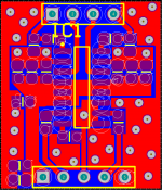
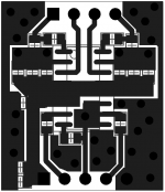
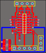
Now, since this chip is such a simple layout, I thought maybe I can do better, which brings me to the real reason for this thread. I have done an initial layout for a PAM stamp, and would like some feedback. I based my layout on the Chinese board, but made several improvements.
1.) Increased input decoupling. Was already fairly good, but can always be better.
2.) Eliminated external 10kR resistor from input, instead relying on input impedence to form the input filter.
3.) Added ground plane everywhere for noise suppression and EMI
4.) Added ferrite bead filter on the output for EMI
5.) Cleaned up the input and output headers (IMO, this is a personal preference thing)
Please note in these photos, the signal input ground should connect to the ground planes surrounding it, I need to fix the copper there. The bottom of the board is a solid ground plane.
Would love to hear the opinion of those with more experience laying out boards, I basically have no clue what I am doing. I will try to get some high res pics of the Chinese board I started with for comparison tomorrow. I can post component values for the passives if anyone wants to know.
10 Pcs PAM8403 2X3W Mini Audio Class D Amplifier Board 2 5 5V Input US SHIP M323 | eBay
Having played with these for a few days now, I can safely say, if you only need a few watts, you will not find a better amplifier for under $1.00. The sound is very good, and the board layout is not terrible. However that is not what this thread is about, just a bit of back story.
After being very satisfied with these I looked into other Diodes inc PAM based amplifiers, and discovered the PAM8406 which is pin compatable, supports down to 2R loads at 5W/ch running 5V. That is all well and good, but you might be saying "I don't use any 2R speakers that will run well at 5W", and you would be correct. The real thing about this chip that caught my eye, was the "mode" selection that the PAM8403 does not have. This chip can be operated in Class AB mode!
After inspecting the layout for the $0.50 boards, I found the mode pin (listed as NC for PAM8403), is already tied to ground, so a simple chip swap will give a PAM8406 amp ready to run in Class AB. So that is what I did, and I can report that it is a fairly significant upgrade from the PAM8403, at the cost of a much lower efficiency.
Now, since this chip is such a simple layout, I thought maybe I can do better, which brings me to the real reason for this thread. I have done an initial layout for a PAM stamp, and would like some feedback. I based my layout on the Chinese board, but made several improvements.
1.) Increased input decoupling. Was already fairly good, but can always be better.
2.) Eliminated external 10kR resistor from input, instead relying on input impedence to form the input filter.
3.) Added ground plane everywhere for noise suppression and EMI
4.) Added ferrite bead filter on the output for EMI
5.) Cleaned up the input and output headers (IMO, this is a personal preference thing)
Please note in these photos, the signal input ground should connect to the ground planes surrounding it, I need to fix the copper there. The bottom of the board is a solid ground plane.
Would love to hear the opinion of those with more experience laying out boards, I basically have no clue what I am doing. I will try to get some high res pics of the Chinese board I started with for comparison tomorrow. I can post component values for the passives if anyone wants to know.
Attachments
Datasheet for those interested
http://www.diodes.com/_files/datasheets/PAM8406.pdf
Switching Freq is 250kHz
Input Impedance is minimum (fixed?) 18kR
I do not have a schematic outside of my head yet, will work on making one tomorrow.
In the mean time, don't hesitate to tear the design apart. I learned a long time ago that when someone starts poking holes in your work, don't get upset, get educated, chances are they know something I don't.
EDIT: I have noticed I accidentally grounded out my right input with my copper pour. oops. I also need to extend pin 12 to connect to the right side ground plane.
Last edited:
Upon discovering that there is a version of the chip available with an exposed thermal pad on the bottom, I may try to rework this board tomorrow to accommodate that package if it can be done cleanly.
Probably not strictly needed, but in Class AB mode the chip does get fairly warm, and that would give me comparability with any version of the chips as well.
This may increase the footprint a bit, as I will probably have to use 1206 bypass capacitors instead of the 0805 in order to get decent thickness output negative traces under them. I will probably also add a jumper to switch between Class D and Class AB.
Mods, feel free to move this thread if you feel it is in the wrong spot.
Last edited:
To me, the actual bypass is kinda "suboptimal", as bypass caps are not in the loop.
Current will mainly go like this:
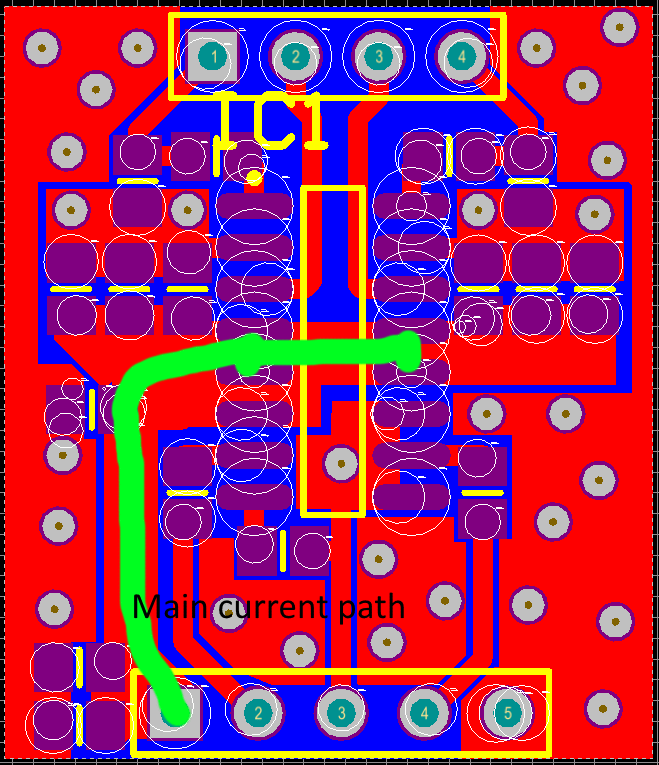
I'd recommend:
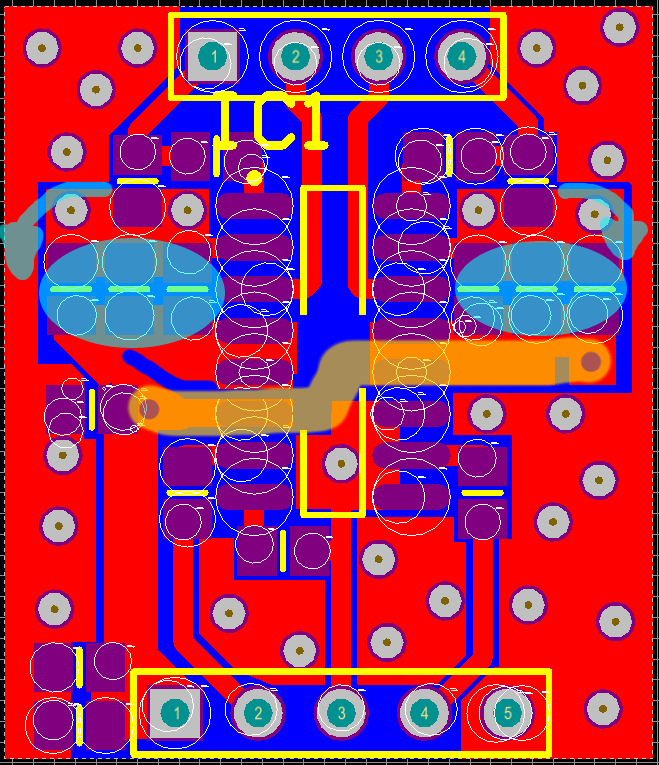
Current should go trough the pads of the caps. "Positive" will face to the chip as close as possible. For this, the caps need to be rotated by 90°. Decoupling per channel/side, so no mid connection of the rail but trace at the bottom to link via Vias. Tracks lead into decoupling "tank" from there to the chip. If needed, reduce to 2 caps per side at the chip, like i.e. 10uF + 100nF. Keep DC-bias in mind, resulting capacitance will be lower
10uF X7R 10V 0805: GRM21BR71A106KE51L
100nF X7R 50V: 0603:
Gives ~6uF at DC-Bias of 5V, should do. Skip the rest and put one "Bulk near the power-input, like 100-330uF 6V3 polymer radial leaded. (non SMD gives lower ESR):
I.e:
150uF 6V3 7mR 5.6A ripple: Nichicon RR70J151MDN1
330uF 6V3 7mR 6.1A ripple: Nichicon RR70J331MDN1
Or if you want it small and smt:
270uF 6V3 14mR 3.14A ripple: Nichicon RSA0J271MCN1GS
180uF 6V3 17mR 3.39A ripple: UCC APXK6R3ARA181ME61G
Done with power decoupling.
Current will mainly go like this:
I'd recommend:
Current should go trough the pads of the caps. "Positive" will face to the chip as close as possible. For this, the caps need to be rotated by 90°. Decoupling per channel/side, so no mid connection of the rail but trace at the bottom to link via Vias. Tracks lead into decoupling "tank" from there to the chip. If needed, reduce to 2 caps per side at the chip, like i.e. 10uF + 100nF. Keep DC-bias in mind, resulting capacitance will be lower
10uF X7R 10V 0805: GRM21BR71A106KE51L
100nF X7R 50V: 0603:
Gives ~6uF at DC-Bias of 5V, should do. Skip the rest and put one "Bulk near the power-input, like 100-330uF 6V3 polymer radial leaded. (non SMD gives lower ESR):
I.e:
150uF 6V3 7mR 5.6A ripple: Nichicon RR70J151MDN1
330uF 6V3 7mR 6.1A ripple: Nichicon RR70J331MDN1
Or if you want it small and smt:
270uF 6V3 14mR 3.14A ripple: Nichicon RSA0J271MCN1GS
180uF 6V3 17mR 3.39A ripple: UCC APXK6R3ARA181ME61G
Done with power decoupling.
Attachments


I started on this for the exposed pad version. Having to route the -OUT traces outside of the IC makes it tricky to place the caps with positive end toward the chip, will have to think about this one.
I have not drawn in ground planes yet, but all via will be ground aside from the 3 connecting to the blue bottom power trace.
I also added jumpers for SHDN, MUTE, and MODE.
I have not drawn in ground planes yet, but all via will be ground aside from the 3 connecting to the blue bottom power trace.
I also added jumpers for SHDN, MUTE, and MODE.
Attachments
One ground-via per cap, even if you do groundfill later. Any reason to have only "half-filter"? EMI is on both outputs, so better go for "full filter". (Ferrite+C)
Pin3/14 directly to ground at thermal pad will free up the "problem" with the caps and routing the outputs.
Because I had misinterpreted the diagram in the 8403 datasheet
") . You are 100% correct that I need filter on both lines.
. You are 100% correct that I need filter on both lines.I assume you mean pins 2 and 15? I wasn't sure if it was proper to go directly to thermal pad ground but since it seems to not be a problem I will do it that way as it does simplify things. Should I tie pin 11 on to TP ground also rather than do an external via?
Yes.I assume you mean pins 2 and 15?
Yes, and route AGND_in on top to thermal-pad only. (coming from your source)Should I tie pin 11 on to TP ground also rather than do an external via?
PGND, coming from the supply, is directly connected to the ground plane.
Understood. Will do those changes, along with proposed changes to capacitance next. Component size will also be dropping down to 0603 for most things as recommended.
I may stick with large package ceramics (1210) for the bulk capacitors in order to keep z-height lower though. Main concern here would be microphonics I think.
I may stick with large package ceramics (1210) for the bulk capacitors in order to keep z-height lower though. Main concern here would be microphonics I think.
Microphonics? That's why you will mount the 1210 90 degrees to the longest board side as deflection is lower on this axis.
You'll have to check if some another MLCC wouldn't be an issue due to massive parallel ceramic. This forms a very high Q which may lead into oscillation. So there might be the need for some small series resistance for the bulk not being right beside the IC. Elythics and Polymer have a bit different Z vs. frequency so they'll filter on the "lower" mid (10-100kHz).
I further wouldn't recommend to use conflict minerals like tantal.
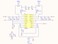
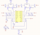
Updated schematic to reflect new filter and decoupling scheme. Also started to fix the layout some, but will be moving the project to KiCAD today so this is all I have for now.
As it is, I know the main VDD pin decoupling is not ideal (read: near useless), but I don't think that is a huge concern as the power amplifier section for each channel has its own decoupling, which is good (I think).
Does the ferrite + C filter need to be located as close to the pins as possible to be effective? I am assuming so which is why the layout is as such, but not certain.
I also need to look into a low profile solution for bulk capacitance that won't cause oscillation (thanks for the heads up). I'm sure some low profile SMD polymers exist. Any reason not to use tantalum aside from the dubious nature of mining the minerals? I won't do so here, but have used them once in the past with good results.
EDIT: Fixed schematic errors
Attachments
Last edited:
These polymer caps look like they would suit the task perfectly, anyone have experience with these?
EEF-CX0J221R Panasonic | Mouser
EEF-CX0J221R Panasonic | Mouser
Beside the usual voltage/temp derating and prone to fire, nope. But being a conflict mineral is reason enough for me, can't speak for others.Any reason not to use tantalum aside from the dubious nature of mining.
https://www.youtube.com/watch?v=CUjhhXILVj0
Yes.Does the ferrite + C filter need to be located as close to the pins as possible to be effective?
Then why not drop it?As it is, I know the main VDD pin decoupling is not ideal (read: near useless), but I don't think that is a huge concern as the power amplifier section for each channel has its own decoupling, which is good (I think).
Kemet T528 series. (very expensive)I also need to look into a low profile solution for bulk capacitance that won't cause oscillation (thanks for the heads up). I'm sure some low profile SMD polymers exist.
Even if the distributors list them as Tantal, Kemet says it's "solid electrolytic
capacitor with a conductive polymer cathode".
Kemet A700 Series
A700V107M006ATE015 100uF 6V3 h=2mm
Panasonic SP-Cap CX Series
EEFCX0J151XR 150uF 6V3 h=1.9mm
----------------
little math, simplified (worst case):
At 6V and 4R load there is 6V/4R= 1.5Apk per side, so 3Apk per amp.
So the PSU needs to deliver 3Apk max. Let's have one EEFCX0J151XR which is 150uF/12mR, time-constant will be R*C = 150uF*12mR = 1.8us. The corner-frequency would be 1/2*pi*ESR*C = 88.5kHz - where XC = R, so at 250kHz there's ~ the 12mR real resistance as the impedance. The residual ripple will be R*Ipk = 12mR*3Apk = 36mVpp. pp because this is BTL.
At 2R load there would be 6Apk per amp, (yeah sure) and Vripple = 72mVpp.
There's nothing we can do about, except lowering the ESR.
------------
Assuming ESR=0, the minimum decoupling capacity at switching frequency (assuming maximum duty-cycle near 1) will be:
C = I * dt/dV
Let's say Vripple should be i.e. 1% of PVCC = 6V*0.01 = 60mV
at 4R load:
Cmin = 3A * 1/250kHz / 60mV = 200uF (at 2R load Cmin = 400uF)
To have Vesrripple = Vripple, ESR needs to be
ESR = Vripple / Ipk = 60mV / 3Apk = 20mR
Normally, ESR ripple will dominate. To have the capacitor ripple <= 10% of the ESR ripple, C needs to be x10, so 2000uF is needed. Taking aging and ESR rise into account, ESR needs to be 30-50% lower than calculated.
So we would need 2000uF at 10mR per amp, when going full power at 4R load and PVCC=6V.
Note:
This worst case calculation is at THD levels well above 10%, so pretty much impractical. Who cares about Vripple at this levels of distortion.
So the practical calculation at "normal" listening levels:
PVCC = 5V
Rload = 4R
THD = 1%
Prms (from datasheet) at this: 2.55Wrms
internal Rdson (combined): 0.32R
Ipk = sqrt(Ppeak / Rload) => Ipk = sqrt((Prms*2)) / (Rload+Rdson))
Ipk = sqrt((2.55W*2) / (4R+0.32R)) = sqrt(3.6W / 4.32R) = 1.09Apk
Ipk_stereo = Ipk*2 = 1.09Apk * 2 = 2.18Apk
Vripple = 1% of PVCC = 50mV
Cmin_stereo = Ipk_stereo * (1/fsw) / Vripple = 2.18Apk * (1/250kHz) / 50mV = 174.4uF
ESR = Vripple / Ipk_stereo = 50mV / 2.18Apk = 23mR
ESR_-50% = 11.5mR
C = Cmin_stereo * 10 = 1744uF
In reality needed capacitance is less, at the levels at 1% THD aren't at nearly maximum duty time.
So 4 * 330uF 46mR caps would do.
Above calculations are for the HF-ripple.
Now what about the low frequencies? If the PSU has an internal DC-resistance of 100mR, our load-current will modulate PVCC at 100mR * 2.18Apk = 0.218V
To compensate for a bass drop of 50ms duration, we can get from C = Q/U => C = Ipk * t / dV
Lets assume, the drop shall be at the level of our maximum Vripple = 50mV (or 1% of PVCC = 5V):
C = 2.18Apk * 50ms / 50mV = 2.18F (farads!)
One could say, we have sine-wave bass and take frequency into account.
So, 50Hz => t = 20ms and Irms = Ipk*0.707 = 1.54Arms
Then to support 1 period at 50Hz:
C = 1.54Arms * 20ms / 50mV = 0.62F
Woohei.
Conclusion:
At listening levels with a crest factor of 6, or x0.5 of Ppeak we can relax even more.
1x1000uF 20mR bulk - done.
And if you feed the the amp by an SMPS, you'll need much less, as there's also the transformated main tank capacitance and lower DC-resistance than 100mR. Would assume 2x330uF Polymer
Switching at the worst case level regarding the driver stage would have losses per side of:
At 4R load and taking Rds_on into account:
Ipk = 6V/(4R + Rds_on_N + Rds_on_P) = 6V/(4R + 0.14R + 0.18R) = 1.39Apk
Rds_on_combined = 0.32R
Power loss per channel:
Peak: (Rds_on_combined) * Ipk^2 = 0.32R * 1.39Apk^2 = 0.62Wpk
RMS: (Rds_on_combined) * (Ipk*0.707)^2 = 0.32R * (1.39Apk*0.707)^2 = 0.31Wrms
So 0.62Wrms per amp. The SOP-16 is stated at Rth_JA = 110°C/W, so junction temp would be:
t_amb + Prms*Rth_JA = 25°C + 0.62Wrms * 110°C*W^-1 = 93.2°C
From another datasheet the Rth_JA for the SOP16_EP is ~45°C/W
so:
t_amb + Prms*Rth_JA = 25°C + 0.62Wrms * 45°C*W^-1 = 52.9°C
At 2R load:
Ipk= 6V/(2R + Rds_on_N + Rds_on_P) = 6V/(2R + 0.14R + 0.18R) = 2.58Apk
Rds_on_combined = 0.32R
Power loss per channel:
Peak: (Rds_on_combined) * Ipk^2 = 0.32R * 2.58Apk^2 = 2.13Wpk
RMS: (Rds_on_combined) * (Ipk*0.707)^2 = 0.32R * (2.58Apk*0.707)^2 = 1.065Wrms
So 2.13Wrms per amp. The SOP-16 is stated at Rth_JA = 110°C/W, so junction temp would be:
t_amb + Prms*Rth_JA = 25°C + 2.13Wrms * 110°C*W^-1 = 259.3°C
From another datasheet the Rth_JA for the SOP16_EP is ~45°C/W
so:
t_amb + Prms*Rth_JA = 25°C + 2.13Wrms * 45°C*W^-1 = 120.85°C
So 2R load wont do continously, for SOP-16.
Maximum Power for Tjunction = 125°C:
Pdiss_rms = (Tjunction - tamb) / Rth_JA
SOP-16:
Pdiss_rms = (125°C - 25°C) / 110°C*W^-1 = 0.9Wrms or 0.45Wrms per channel
Ipk = sqrt(Pdiss_rms) / (sqrt(Rds_on_combined) * 0.707)
Ipk = sqrt(0.45Wrms) / (sqrt(0.32R) * 0.707) = 1.677Apk per channel
SOP-16-EP:
Pdiss_rms = (125°C - 25°C) / 45°C*W^-1 = 2.22Wrms or 1.11Wrms per channel
Ipk = sqrt(Pdiss_rms) / (sqrt(Rds_on_combined) * 0.707)
Ipk = sqrt(1.11Wrms) / (sqrt(0.32R) * 0.707) = 2.63Apk per channel
Conclusion (thermal max cont. peak/rms output power per channel):
SOP-16:
Peak: 4R load: 1.677Apk^2 * (4R+0.32R) = 12.15Wpk
RMS: 4R load: (1.677Apk*0.707)^2 * (4R+0.32R) = 6.07Wrms
Peak: 2R load: 1.677Apk^2 * (2R+0.32R) = 6.52Wpk
RMS: 2R load: (1.677Apk*0.707)^2 * (2R+0.32R) = 3.26Wrms
SOP-16-EP:
Peak: 4R load: 2.63Apk^2 * (4R+0.32R) = 29.88Wpk
RMS: 4R load: (2.63Apk*0.707)^2 * (4R+0.32R) = 14.94Wrms
Peak: 2R load: 2.63Apk^2 * (2R+0.32R) = 16.05Wpk
RMS: 2R load: (2.63Apk*0.707)^2 * (2R+0.32R) = 8.025Wrms
Note: Ipk is limited by PVCC/Rload+Rdson.
Correct me if i'm wrong.
Whew! Alright, so if I understand this correctly, I need (roughly) 1000uF to maintain a ripple of less than 1% at not quite worst case conditions, and could probably get away with less. I think I will plan to use the Panasonic caps for now, but those Wurth you posted are tempting at that price.
It also looks like I will in fact need to use the SO16-EP package if I plan to use 2R (I dont,right now, but I would like the option to be open). I had done some back of the envelope calculations on thermals prior which is how I decided to use the EP version, glad it has been confirmed.
Thanks so much for taking the time, I appreciate all the help, have learned quite a lot already.
Regarding Tantalum. Fire? Never! They don't damn near explode when you accidentally hook them up with reverse polarity or anything (sarcasm). I didn't realize it was a conflict mineral until after you had mentioned it though, I went and looked it up, thanks for the heads up, will avoid using it in the future.
EDIT: Worth noting, power supply right now is a AC to USB adapter capable of 2.4A. Being as these are 5V devices though, if an actual USB cable is used, series resistance with the supply might actually be a problem with the thinner cables.
It also looks like I will in fact need to use the SO16-EP package if I plan to use 2R (I dont,right now, but I would like the option to be open). I had done some back of the envelope calculations on thermals prior which is how I decided to use the EP version, glad it has been confirmed.
Thanks so much for taking the time, I appreciate all the help, have learned quite a lot already.
Regarding Tantalum. Fire? Never! They don't damn near explode when you accidentally hook them up with reverse polarity or anything
(sarcasm). I didn't realize it was a conflict mineral until after you had mentioned it though, I went and looked it up, thanks for the heads up, will avoid using it in the future.EDIT: Worth noting, power supply right now is a AC to USB adapter capable of 2.4A. Being as these are 5V devices though, if an actual USB cable is used, series resistance with the supply might actually be a problem with the thinner cables.
Last edited:
Possible/Only fix: Use proper/no cable, because not only Rcable but also Lcable will have an impact. While the first limits your PVCC at load, the latter will limit your dI/dT. You can't do much about that for low frequencies, as shown from the math. For the rest, calculate the corner-frequency of the decoupling caps.... if an actual USB cable is used, series resistance with the supply might actually be a problem with the thinner cables.
Beside that, with 1000uF Polymer combined + the 10uF MLCC per side you're actually better than most "low cost" TI boards. (We're talking about < 2x5W)
Worth to note: You can't count on much primary capacitance within this small USB-supplies. Let there be 47uF primary at rectified 110V*sqrt(2) = 155Vdc and Q = C * U = 47uF * 155V = 7.3mAs. Transformed to secondary at "ideal": C = Q/U = 7.3mAs/5V = 1460uF - not taking any losses into account. (+ secondary bulk at psu)
Last edited:
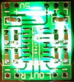
Brief intermission to check out the "competition" (inspiration?). The passives are all 1uF aside from the 4.7uF "bulk" capacitor at the bottom left.
10k input resistors for the input filter, probably because the schematic in the datasheet shows them external, but really you can use the 18k input resistance of the chip.
With all that, it does sound pretty good, so really I am just over engineering everything for my own learning. Will be interesting to listen to both side by side when I am done though. Wish I had the equipment to actually measure them.
May or may not have an updated layout tomorrow, as I am learning to use KiCAD, so much different than what I am used to.
Attachments
You may want think over what will happen when you use that amp without external gain resistor. (Which will give 24dB gain or factor 15.85) At PVCC=5V max rms output amplitude would be 3.53Vrms so your clipping input rms is then 3.53Vrms / 15.85 = 0.223Vrms. Normal mobile output is ~1Vrms.
Wouldn't a factor of 3.5-4 be better? (10-12dB)
Wouldn't a factor of 3.5-4 be better? (10-12dB)
Last edited:
- Home
- Amplifiers
- Class D
- PAM8406 (and PAM8403)