some DIP comparators with <30ns propagation delay
The first is the cheapest.
LM306
AD8561
LT1016
MAX903
TL3016 from TI. Works well for me and has slightly improved parameters over the LT1016 (with which it is pin compatible).
TL3016 from TI. Works well for me and has slightly improved parameters over the LT1016 (with which it is pin compatible).
TL3116 is much better with common mode range extending to negative rail.
")
I have thought about some way to control the hysteresis: Markus and I were already in contact privately about this and I will try to sim it and if it "works" I will post details.
I don't know however, wheter soemeone else has already used the same principle already. One can never be sure nowadays - just make a patent search for class-d and you'll know what I mean.
Regards
Charles
I don't know however, wheter soemeone else has already used the same principle already. One can never be sure nowadays - just make a patent search for class-d and you'll know what I mean.
Regards
Charles
TL3116 is much better with common mode range extending to negative rail.
Thanks Workhorse, I wasn't aware of that one. I use the TL3016 with +/-5V supplies so the c-m range isn't all that important, but the 3116 might be useful in the future.
Great !
This sort of busy thread is making me feel better.
...ohps and is bringing me to the situation that I might not be able to handle all input properly....
@manojtm:
I am also wondering why a totem pole driver should cause noise.
Have a look to posting #27. The figures there are all derived with an amp design that uses a BJT totem pole gate drive.
Ok the MosFets there were just half as heavy as the IRFP4668, but still heavy.
IRFB4115 driven from FTZ853/953 and IRS20957.
IMHO the noise figures are far better than average.
Do you have even higher spec demands? I mean, I need a headphone plugged directly to the speaker output in order to hear the noise at all.
I don't think that totem pole drivers cause generally noise, but it would be interesting to dig for the very detailed trouble mechanism, which caused issues in your experience. Such know how avoids to get trapped by the same pit falls.
Could it be that the faster switching caused more HF-ringing and in consequence more NF-noise? I am seeing in your design from the 25-1200 thread, extremely slow gate drive, which most likely is good for EMI and will also calm down the HFjunk-to-NFnoise conversion of the comparator, but most likely such slow switching impacts THD.
With this thread here, I am not aiming for THD levels as in posting #27, but I don't want to worsen it more than 20db. And idle noise should not worsen more than 10db.
The downside of faster switching is that you cannot get away with mini snubbers. I am sure that I cannot go with such light snubbers as your design. I am expecting more that I need 1nF and something between 5-10 Ohms. ...and of course will have to live with about 1.5W snubber losses.
LM306: PropDelay is 28ns. Stoneagedesign. I like it. Available in DIP8 at DigiKey.
AD8561: To much of high speed high end. But at least available at as DIP8 at DigiKey.
LT1016: Also faster than I love. Available as DIP8 at DigiKey, Bürklin and Reichelt.
Max903: Again pretty fast, TTL output, not available at any of my daily sources.
TL3016/3116: Again very fast, not available in DIP8 at all, SMD available at Digikey.
My favorites would be LM306 and LT1016. Unfortunately they have pretty different PIN connections.
Any comments on personal taste and availability in other parts of the world?
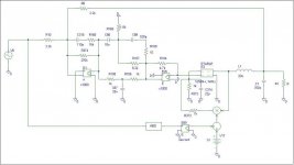
The floating input stage of the IRS20957 does not need to be connected to GND. It could also be bound to -8.25V in example.
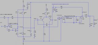
This would allow an ultra simple discrete comparator as shown in the attached schematic. Not sure if this thing already deserves the name comparator, but basically it seems to work reasonably good even with standard components.
The low gain causes an additional delay. With the concerned signals it takes about 60ns until the differential input signal is large enough to generate a comparator output which crosses the flipping point of the IRS input (comp out ramps in approx 120ns).
Impact on idle frequency is still moderate (less than 10kHz).
I have to check for impacts on performance like distortion and frequency control by dynamic hysteresis....
Don't wonder about my strange voltages like 1.65V, 3.3V or 8.25V.
They can easily be derived from a chain of red LEDs ==> low noise zener substitute.
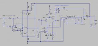
An upgrade with much more comparator gain could be the second schematic, still I am not convinced that the extra efforts are worth it. But it simulates nice. Sloping with the concerned input signals takes 30ns, delay just a few ns (hard to believe).
Please also note the inspiration from Workhorse combined with my improvement to move the mirror to a neg voltage and clamping which avoids saturation of the BJTs.
This would allow an ultra simple discrete comparator as shown in the attached schematic. Not sure if this thing already deserves the name comparator, but basically it seems to work reasonably good even with standard components.
The low gain causes an additional delay. With the concerned signals it takes about 60ns until the differential input signal is large enough to generate a comparator output which crosses the flipping point of the IRS input (comp out ramps in approx 120ns).
Impact on idle frequency is still moderate (less than 10kHz).
I have to check for impacts on performance like distortion and frequency control by dynamic hysteresis....
Don't wonder about my strange voltages like 1.65V, 3.3V or 8.25V.
They can easily be derived from a chain of red LEDs ==> low noise zener substitute.
An upgrade with much more comparator gain could be the second schematic, still I am not convinced that the extra efforts are worth it. But it simulates nice. Sloping with the concerned input signals takes 30ns, delay just a few ns (hard to believe).
Please also note the inspiration from Workhorse combined with my improvement to move the mirror to a neg voltage and clamping which avoids saturation of the BJTs.
Attachments
...good point with the BSS - must have something like this somewhere in my component boxes....
Idle frequency is 380kHz, with the shown hysteresis and delays (in theory/simulation). But I trust that the delays are more or less realistic.
In SystemD_MD I have 140ns delay from IRS-input to halfbridge output, so 230ns with the IRFP4668 is already a slow guess, I think/hope it will be faster which would ask for a slightly larger hysteresis to fit the same idling frequency and would allow even better control of the frequency by the dynamic hysteresis.
Dynamic hysteresis control
Here you can see a simulation model of my proposal. It uses a 2nd order feedback loop with post-filter feedback as general topology.
It would of course also work with pre-filter or other post filter topologies (than the one shown here).
Because it is only a simulation model with an output voltage of +- 1 V the "comparator and the output stage is the same (maybe it would have been better to separte them for clarity).
With a real implementation one would take the positive feedback for the hysteresis from the comparator and the NFB from the power output.
The hysteresis is controlled by modulating a reference voltage. This voltage is the actual voltage that is positively fed-back (to cause the hysteresis). The multiplier is actually just acting as a polarity switch. I.e. the reference voltage is either inverted or not - depending on the output state of the comparator.
In practice one would implement this "multiplier" either with a CMOS analog switch that is controlled by the comparator output voltage (and which is switching between a positive and a negative reference voltage) or by modulating the supply voltage of a CMOS -buffer/-levelshifter whose input is connected to the comparator output.
The amount of hysteresis is then controlled by subtracting a voltage - that is dependant on the input voltage of the amp - from the reference voltage. In this example here the subtracted voltage is directly proportional to the input amplitude. A deeper analysis would be needed in order to find out whether a different mathematical function (or just a coarse approximation of such a function) than just proportional would be advantageous. A practical circuit would also need some additional simple means to tame the hyteresis control under overload conditions.
I don't know whether something like this has already been patented. If not - maybe heaps of amps using it may pop up from China quickly
For the impatient ones:
If driven to around 10% of max outpult voltage the influence on THD (which is low in this situation anyway) is benign, at 90% drive it means a THD improvement of about tenfold. But these are simulations and have to be taken with the usual grain of salt of course.
Regards
Charles
Attachments
Great! - now I have to think and cannot comment immediately...
In order to get my brain free to think about Charles' version,
first an update on the comparator topic.
The ultra simple comparator is doing a fairly good job in simulation.
From data sheet of IRS20957 I came to the conclusion that it would
be better to shift the floating input stage towards positive, because
VSS must not be pulled below COM. In case of missing high power rails
COM is likely to be equal with GND and in this case putting VSS to -8V is not allowed. Clamping by a diode is ugh, because this would then pull the -8V towards GND...
So shifting VSS some volts towards positive is better - and also possible with a triple-BJT-comparator.
Nevertheless I am intending to use integrated comparators - just because of component count and number solder joints. The headaches for debugging a new built grow proportional with the number of solder joints and exponential with the number of components. Adding up my debugging times when building SystemD_MD (317 components, unbridged) is likely to sum up to a full day for debugging only.
Impossible to transfer such a design to other DIYers, except the ones who could design it on their own anyway.
I definitely want to avoid that this happens to SystemD_2kW.
Many thanks for all your proposals of comparators.
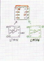
I think there is a simple way to set a PCB which allows LT1016 and LM306.
Depending on personal taste and availability one or the other can be placed.
Have a look to the attached sketch, which is showing one possible PCB solution for both (final solution will depend on the very layout details).
Well, allowing this flexibility again generates additional chances to build something wrong, but I think it is easy to handle and worth the flexibility.
In order to get my brain free to think about Charles' version,
first an update on the comparator topic.
The ultra simple comparator is doing a fairly good job in simulation.
From data sheet of IRS20957 I came to the conclusion that it would
be better to shift the floating input stage towards positive, because
VSS must not be pulled below COM. In case of missing high power rails
COM is likely to be equal with GND and in this case putting VSS to -8V is not allowed. Clamping by a diode is ugh, because this would then pull the -8V towards GND...
So shifting VSS some volts towards positive is better - and also possible with a triple-BJT-comparator.
Nevertheless I am intending to use integrated comparators - just because of component count and number solder joints. The headaches for debugging a new built grow proportional with the number of solder joints and exponential with the number of components. Adding up my debugging times when building SystemD_MD (317 components, unbridged) is likely to sum up to a full day for debugging only.
Impossible to transfer such a design to other DIYers, except the ones who could design it on their own anyway.
I definitely want to avoid that this happens to SystemD_2kW.
Many thanks for all your proposals of comparators.
I think there is a simple way to set a PCB which allows LT1016 and LM306.
Depending on personal taste and availability one or the other can be placed.
Have a look to the attached sketch, which is showing one possible PCB solution for both (final solution will depend on the very layout details).
Well, allowing this flexibility again generates additional chances to build something wrong, but I think it is easy to handle and worth the flexibility.
Attachments
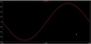
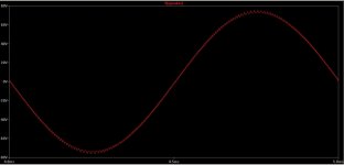
So here are the sims.
Keep in mind that the improvement will most probably be better as soon as the phase-lag between the amp input and the input to the modulator is taken into consideration as well. The gain of E87 was set to 0.7 when dynamic control was enabled.
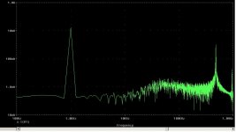
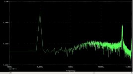
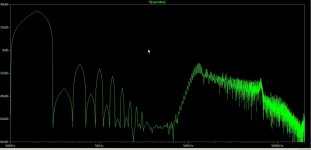
The graphics show the following:
Output spectrum with 10% drive at 1 kHz and dynamic control disabled.
Dito with dynamic control enabled -> not a big difference.
Output spectrum with 90% drive and dynamic control disabled.
The same with dynamic control enabled - at least 20 dB improvement in THD and a clear restriction of the frequency range that is swept by the switching frequency. Not so elegant is the ratio between k3 and k5.
Output signal without dynamic hysteresis control at 90% drive.
The same with hysteresis control enabled.
Regards
Charles
Keep in mind that the improvement will most probably be better as soon as the phase-lag between the amp input and the input to the modulator is taken into consideration as well. The gain of E87 was set to 0.7 when dynamic control was enabled.
The graphics show the following:
Output spectrum with 10% drive at 1 kHz and dynamic control disabled.
Dito with dynamic control enabled -> not a big difference.
Output spectrum with 90% drive and dynamic control disabled.
The same with dynamic control enabled - at least 20 dB improvement in THD and a clear restriction of the frequency range that is swept by the switching frequency. Not so elegant is the ratio between k3 and k5.
Output signal without dynamic hysteresis control at 90% drive.
The same with hysteresis control enabled.
Regards
Charles
Attachments
Hi Charles,
....I think I got it. That's nice. And your sim results are looking pretty nice.
You are not just controlling the hysteresis in order to avoid massive voltage ripple at high output levels - you vary the hysteresis over a large voltage range in order to optimize distortion and avoid massive voltage ripple at the same time.
I did not compare distortion at 90% with and without dynamic hyteresis in my approach. ==> coming soon (one day off today )
Furtheron I have to check if I can parametrize to optimize for this dual functionality in my implementation as well. Great input!
But let's stick with your proposal of implementation.
As already visible in my previous posting - for this project I am acting like a "Erbsenzähler" (English: Nitpicker) in terms of component count and solder joints.
I even considered to skip the triangle shaping and dynamic hysteresis - but no, that would be to poor!
ABS:
5x resistor
1x dual OP amp
2x supply cap for dual OP amp
E89:
As long as we stay with the proportional approach, this gain can be incorporated into the ABS circuit.
Reference:
For sure something reasonable available without additional effort (i.e. pick from LED chain...)
Substractor:
1x OP amp
2x supply cap for OP amp
4x resistor
Multiplier (Buffer with modulated supply):
6x resistor
1x dual OP amp
2x supply cap for dual OP amp
1x buffer
2x supply cap for buffer (RC between OP amp and supply pin of buffer)
2x resistor (RC between OP amp and supply pin of buffer)
1x summing resistor towards hysteresis
OverloadCircuit:
?
Hm, overall not to bad, but already extensive.
Basically I would prefer to use the CMOS-Switch-Multiplier, but from my understanding we would not get right the polarity information from the PWM signal.
The analogue input of the CMOS-Switch is needed to make use of the analog information from the substractor.
So only the ON/OFF input of the CMOS can be used for the PWM information... -or do I miss something?
P.S.
...looks like your control loop also incorporates a shaped D portion..
....I think I got it. That's nice. And your sim results are looking pretty nice.
You are not just controlling the hysteresis in order to avoid massive voltage ripple at high output levels - you vary the hysteresis over a large voltage range in order to optimize distortion and avoid massive voltage ripple at the same time.
I did not compare distortion at 90% with and without dynamic hyteresis in my approach. ==> coming soon (one day off today
) Furtheron I have to check if I can parametrize to optimize for this dual functionality in my implementation as well. Great input!
But let's stick with your proposal of implementation.
As already visible in my previous posting - for this project I am acting like a "Erbsenzähler" (English: Nitpicker) in terms of component count and solder joints.
I even considered to skip the triangle shaping and dynamic hysteresis - but no, that would be to poor!
ABS:
5x resistor
1x dual OP amp
2x supply cap for dual OP amp
E89:
As long as we stay with the proportional approach, this gain can be incorporated into the ABS circuit.
Reference:
For sure something reasonable available without additional effort (i.e. pick from LED chain...)
Substractor:
1x OP amp
2x supply cap for OP amp
4x resistor
Multiplier (Buffer with modulated supply):
6x resistor
1x dual OP amp
2x supply cap for dual OP amp
1x buffer
2x supply cap for buffer (RC between OP amp and supply pin of buffer)
2x resistor (RC between OP amp and supply pin of buffer)
1x summing resistor towards hysteresis
OverloadCircuit:
?
Hm, overall not to bad, but already extensive.
Basically I would prefer to use the CMOS-Switch-Multiplier, but from my understanding we would not get right the polarity information from the PWM signal.
The analogue input of the CMOS-Switch is needed to make use of the analog information from the substractor.
So only the ON/OFF input of the CMOS can be used for the PWM information... -or do I miss something?
P.S.
...looks like your control loop also incorporates a shaped D portion..
The "analog" part of a CD4053 (3x 2 channel multiplexer or just atoggle switch IMHO) can be run from symmetrical suplies and handle negative voltages whil the input control is done with H = Vdd and L = Vss.
But you would need to make a negative mirror image of the reference voltage as well. I.e. one more OP-AMP plus two resistors plus means for decoupling.
Regards
Charles
But you would need to make a negative mirror image of the reference voltage as well. I.e. one more OP-AMP plus two resistors plus means for decoupling.
Regards
Charles
Hi,
Congratulations to you two, this is the right way to play well in a class D.
In particular, the idea of Charlie is very similar to that used by me. (I also control a proportion value of the audio frequency), voltage control is also reported to the frequency audio I mean. (my DXA use just a similar concept)
This system also, delete the errors added in the modulator when applying a scheme of nfb, such as self-oscillating post-filter feedback.
Regards
Not sure - I simulated with symmetrical hysteresis. Maybe it works as well when each control voltage is just derived from either half-wave of the input signal. Although I somehow don't like it. and you would need two half-wave rectifiers which wouldn't lower parts-count much.
Regards
Charles
Regards
Charles
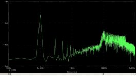
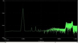
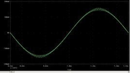
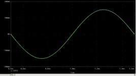
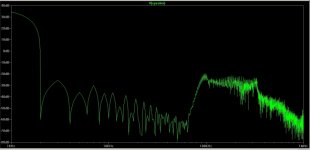
I took my simulation - values and schematic circuit according the posting #3 and #14 - and checked the influence of the dynamic hysteresis on the harmonics at 90%.
Also in this circuit the dynamic hysteresis is helpful for harmonics at high levels. Already unmodified it improves the situation about 15db. Not sure if it can reach identical results as Charles' solution, just by optimized parameters, but already 15db positive effect is nice.
This result is fitting to the obvious effect that the shape of the feedback carrier turns less and less triangular the more the frequencies drops.
Many thanks to Charles for pointing to this.
1. Output shape with constant hysteresis
2. Output shape with dynamic hysteresis
3. FFT with constant hysteresis
4. FFT with dynamic hysteresis
Attachments
- Home
- Amplifiers
- Class D
- SystemD_2kW, any interest for an open design?