Hello,
I've been working on a class D amplifier design (single channel) which I've split into modules so that I could experiment with different modulators and MOSFET drivers:
I'm considering making the PCB and design files available for people to experiment with and want to gauge interest to see if anyone is interested.
Thanks.
I've been working on a class D amplifier design (single channel) which I've split into modules so that I could experiment with different modulators and MOSFET drivers:
- Power Board - contains the high power circuitry (MOSFETS and associated bias circuitry) and output filter (several stuffing options available for the output filter). MOSFET drivers are on a separate daughter board.
- MOSFET Driver Boards - My design uses discrete drivers, but other boards could be made using commercial driver chips.
- Modulator Board - Preamp + modulator + protection circuitry. The current design uses a fully differential LME49990 based front end, UCD style modulator, and protection from over/under supply, DC on output, and overcurrent.
I'm considering making the PCB and design files available for people to experiment with and want to gauge interest to see if anyone is interested.
Thanks.
I'm still prototyping the amp, so the design isn't quite final yet, but here are some pictures. I can post the current schematics if there is interest.
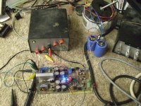
1) Overall picture with toroid supply and the amp board set.
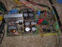
2) Power board on left, signal board on right.
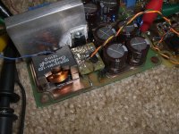
3) Close up of power board showing the small driver daughter cards. The twisted wire leaving the daughter card is part of the overcurrent detection and has been added to the power board on the latest revision.
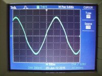
4) Scope capture at the speaker output terminals with no audio signal. The "carrier" is about 1Vpeak-to-peak, 338Khz. The switching transients can be seen but are quite small.
As for the sound, since I've only got one channel completed at the current time, all I can say is that so far, it has a powerful, clean sound. I'm running about 125W RMS into 8ohms.
1) Overall picture with toroid supply and the amp board set.
2) Power board on left, signal board on right.
3) Close up of power board showing the small driver daughter cards. The twisted wire leaving the daughter card is part of the overcurrent detection and has been added to the power board on the latest revision.
4) Scope capture at the speaker output terminals with no audio signal. The "carrier" is about 1Vpeak-to-peak, 338Khz. The switching transients can be seen but are quite small.
As for the sound, since I've only got one channel completed at the current time, all I can say is that so far, it has a powerful, clean sound. I'm running about 125W RMS into 8ohms.
Attachments
I really enjoy to see such DIY, which is not just a blind copy.
The remaining switching transients at the output are really neglectible.
Close to perfect IMHO. How does your output filter look in detail? Circuit, caps, layout details?
BTW:
Please do me a favor and generally put something fire retarding below power electronics.
Preferred stone plates, or ceramic plates - even wood is better than the carpet.
Carpets tend to act like BBQ charcoal lighters.
Except for the modulator, the design is original. I tried to build a class-D amp 20 years ago while I was in high school. The amp worked - sort of. Now that I understand a lot more about high current design, I figured I'd try again.
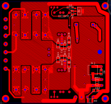
I've attached screenshots of the power board layout and the schematic. One of the key elements of the power board is the area between the two mosfets (approx. in the middle of the board). The really fast switching is going on here - both MOSFETs and the decoupling caps are located within 1cm of each other. The main electrolytic caps are mounted on the left side. I use four for each power rail - it's probably overkill, but I like it that way.
The final attachment is the signal board schematic. There you can see the modulator and various protection circuits. The current design has the following protections:
1) Under voltage - both rails must be >30v
2) Over voltage - since this is currently a single end design, bus pumping can occur. If either rail exceeds 65v, the amp will shut down until the rail recovers to 60v.
3) DC on output. A servo circuit is used to maintain DC balance on the output. This serves two purposes:
- Deals with offsets in the modulator
- Handles the case where the audio-in contains small amounts of DC
If the servo can't correct the DC on the output, the amp will be disabled to prevent speaker destruction.
All of the error outputs are available on the terminal block (J14) so that the amp builder can provide status LEDs on the front panel and possibly to shut down the power supply in case of DC on output. Also on J14 is an input which, if pulled to ground, will shut down the amp.
Attachments
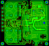
One of the key elements of the power board is the area between the two mosfets (approx. in the middle of the board). The really fast switching is going on here - both MOSFETs and the decoupling caps are located within 1cm of each other.
IMHO that's the critical area were most DIYers fail and spoil all efforts with catastrophic resonances caused by an unfortunate layout of the switching stage.
Your arrangement is definitely looking like one of the better solutions.
Frankly speaking one of the top-routings, that I have seen.

Thanks (Prost!). I've spent a lot of time understanding which parts of the layout need extreme care and which are less important. In that critical area between the two MOSFETs, you are dealing with 50-100Mhz design. Once you leave that small space, suddenly you're in the 300Khz realm and things get a lot easier in terms of parasitic inductance. I've tried to keep the loop area small in this area as well; keeping the traces entering and exiting the main inductor as close as possible. I understand that this may cause some capacitive coupling, but as the scope trace shows, it appears quite minimal.
This is one nice platform here!
Several comments:
1. Transients are mainly filtered by the second LC filter I guess, the main inductor looks pretty capacitive and bulky film cap is rather inductive. On the other hand, the second LC filter is likely to exceed some carrier hamonics now and then, which may increase THD with carrier-based variable frequency schemes, like UcD. Indeed, the scope shot of the carrier you've provided looks like having plenty of 5th harmonic.
2. 4x100uF/100V is everything but overkill, a single cap will have ripple rating of some 0.5A, if you're lucky. The combined ESR is deifinetely higher than mosfets' Rdson.
3. Are you SMDing TO-220's?
4. What's the 'feedback' resistors to the gates for?
Anyway, it's been a pleasure to see someone understanding class-D layout techniques and doing things properly!
To answer the questions:
1) I'll come back to this one at a later time when I can answer more thoroughly.
2) I haven't seen four caps on other designs, but I wanted to stay well within the ripple ratings. Yes, you can exceed the ratings for a while, but things get hot and maybe go boom! I believe the caps I used were rated for 750mA each.
3) Yes, I am SMD mounting the TO-220s to further reduce inductance. I'm not sure the hassle was worth it. In the layout, each MOSFET has a one through-hole to the power on the other side of the board. The gate and drain connect to the top layer.
4) Since this is a modular design, with removable driver boards, the 33k "feedback" resistors are really meant to keep the MOSFETs from accidentally turning on (and smoking - Ask me how I know!) when the driver board is removed - otherwise they have no function.
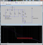
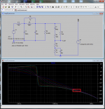
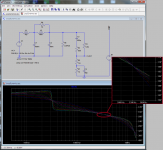
Ok, here's what I'm doing with the dual inductor setup in my amp. I sat down with the simulator and ran three simulations. All three take into account the propagation delay of 107nS through my modulator. The load resistance is swept from 1ohm to 100ohms. The circuit will oscillate at the frequency where the phase crosses 180 degrees. My goal was to make the frequency as independent of load as possible:
1) No lead compensation - the frequency varies from 50Khz to 400Khz
2) Lead compensation found in UcD - from 300 to 500 Khz. Of course, tuning the compensation network can give better results than my simulation.
3) Dual inductor filter - Adding the 2nd inductor (in the simulations by changing R9 to 10 ohms from a short circuit) causes the phase lines to converge at a single point. By adjusting the lead compensation, I can force that point to 180 phase shift. The result is impressive - on my amp, only 5Khz change from 1ohm to open circuit.
Of course, I only know enough to be dangerous. I wish my math skills could understand my experimental findings.
Attachments
Except for the modulator, the design is original. I tried to build a class-D amp 20 years ago while I was in high school. The amp worked - sort of. Now that I understand a lot more about high current design, I figured I'd try again.
I've attached screenshots of the power board layout and the schematic. One of the key elements of the power board is the area between the two mosfets (approx. in the middle of the board). The really fast switching is going on here - both MOSFETs and the decoupling caps are located within 1cm of each other. The main electrolytic caps are mounted on the left side. I use four for each power rail - it's probably overkill, but I like it that way.
The final attachment is the signal board schematic. There you can see the modulator and various protection circuits. The current design has the following protections:
1) Under voltage - both rails must be >30v
2) Over voltage - since this is currently a single end design, bus pumping can occur. If either rail exceeds 65v, the amp will shut down until the rail recovers to 60v.
3) DC on output. A servo circuit is used to maintain DC balance on the output. This serves two purposes:
- Deals with offsets in the modulator
- Handles the case where the audio-in contains small amounts of DC
If the servo can't correct the DC on the output, the amp will be disabled to prevent speaker destruction.
All of the error outputs are available on the terminal block (J14) so that the amp builder can provide status LEDs on the front panel and possibly to shut down the power supply in case of DC on output. Also on J14 is an input which, if pulled to ground, will shut down the amp.
Magnificent contribution.
")
I congratulate you, for sharing.
- Status
- This old topic is closed. If you want to reopen this topic, contact a moderator using the "Report Post" button.
- Home
- Amplifiers
- Class D
- Class D Development Platform