A year ago, when I set out to bring myself up-to-date with Class-D amplifier designs, this DIYaudio forum was a great help. It has been 35 years since I last researched and published Class D and Class E output circuit designs, and the new audio power amp chips were exactly what I needed for a new system I am building, based around a MiniDSP and my bi-amped "ground effect omnidirectional" speaker design.
But one thing which was lacking here was detailed information on available output filter technologies and components. It seems as though much of the technology produced in the '70s has disappeared into the mists of time. So I decided to document my deliberations, and make the design available for all DIYaudio members.
I couldn't buy any 'reference' TDA7498 circuit boards, so I bought a few SURE Electronics boards from Ebay, ripped out the key components, optimized them, soldered in the latest surface-mount TDA7498 chips from Mouser, and started working on today's design issues.
The previous threads I have started here have gotten quite messy in the handling of images, so I decided to put up the complete 'tutorial' on my personal website, and duplicate any key material here. I would also be happy to answer the technical questions that members may have.
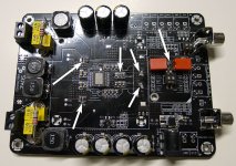
I started by reducing the SURE board's distortion at high frequencies by ten times. From 3% to 0.3%. By changing just two components on the board. But you can see on the photo below the full set of changes I made to the SURE assemblies before I was happy with them")
The result has been to make my SURE TDA7498 assemblies into top-notch (IMO), clean, powerful audio amplifiers. More than adequate for the compact HiFi speakers they are intended to match.
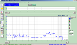
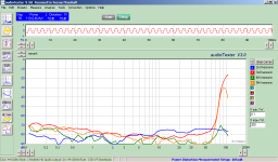
The leftmost attachment is the (final) modded board (without the heatsink) with the measured 8 ohm THD vs frequency curve next to it, followed by the distortion vs power-out curve. Note that I have separated the second, third, fourth and fifth harmonic distortions on the power-out curve to make it easier to see the interplay between even and odd harmonics.
The complete tutorial is on my website at Trevor Marshall - Class D Audio Amplifier Design - TDA7498 Output filters
This output filter topology will work equally well with most of the new >50W bridged amp chips now in the market.
Happy New Year to one and all....
.
But one thing which was lacking here was detailed information on available output filter technologies and components. It seems as though much of the technology produced in the '70s has disappeared into the mists of time. So I decided to document my deliberations, and make the design available for all DIYaudio members.
I couldn't buy any 'reference' TDA7498 circuit boards, so I bought a few SURE Electronics boards from Ebay, ripped out the key components, optimized them, soldered in the latest surface-mount TDA7498 chips from Mouser, and started working on today's design issues.
The previous threads I have started here have gotten quite messy in the handling of images, so I decided to put up the complete 'tutorial' on my personal website, and duplicate any key material here. I would also be happy to answer the technical questions that members may have.
I started by reducing the SURE board's distortion at high frequencies by ten times. From 3% to 0.3%. By changing just two components on the board. But you can see on the photo below the full set of changes I made to the SURE assemblies before I was happy with them
The result has been to make my SURE TDA7498 assemblies into top-notch (IMO), clean, powerful audio amplifiers. More than adequate for the compact HiFi speakers they are intended to match.
The leftmost attachment is the (final) modded board (without the heatsink) with the measured 8 ohm THD vs frequency curve next to it, followed by the distortion vs power-out curve. Note that I have separated the second, third, fourth and fifth harmonic distortions on the power-out curve to make it easier to see the interplay between even and odd harmonics.
The complete tutorial is on my website at Trevor Marshall - Class D Audio Amplifier Design - TDA7498 Output filters
This output filter topology will work equally well with most of the new >50W bridged amp chips now in the market.
Happy New Year to one and all....
.
Attachments
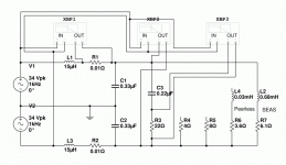
Glad you found it useful. I have now updated my webpage with the MultiSim simulation file, so you can replicate my results, and explore the design issues in more detail. The schematic is attached below.
I have placed 0.01 ohm resistors in series with the inductors to allow me to plot the inductor (and FET switch) currents. There are three Bode plotting instruments, XBP1 for the inductor current, XBP2 for the output voltage vs frequency response, and XBP3 to show the voltage across the damping resistance, and hence allow its power dissipation to be calculated. A compromise has to be struck between power dissipated in this resistor at high frequencies, and the damping applied at the filter resonance. In this case, I decided to ensure that the peak current was just within the capabilities of the FET switches in a good TDA7498 (7 amps typ.)
The direct link to the simulation file is:
http://trevormarshall.com/class-d-tutorial/Trevmar_output_filter.ms11
.
Attachments
I find your work very interesting. I think you show that the output filter is the greatest problem with class-d amps and is the reason reviews of class-d amps vary so widely. The sound changes with different speakers more than almost any other amp due to the output filter. Your dummy load graphs show how the highs vary with load, and this is very audible. I am ignorant of how changing the capacitor type can cause the distortion to go down. Do you know what the mechanism is? I can hear the difference between capacitor types (subtle, yes), but some people see the whole thing as "snake oil".
Would you do me a favor, and honor, by looking at my recent post entitled "Class-D Output Filter - A Case Study". My aim is to show how DIYers can greatly improve their class-d amps just by designing the output filter to match their own speakers. It is fairly easy, you only need to measure the DC impedance and inductance of your high freq driver, and solve the equations.
Would you do me a favor, and honor, by looking at my recent post entitled "Class-D Output Filter - A Case Study". My aim is to show how DIYers can greatly improve their class-d amps just by designing the output filter to match their own speakers. It is fairly easy, you only need to measure the DC impedance and inductance of your high freq driver, and solve the equations.
You may be able to keep the class-d board inductor and let the cutoff freq change by changing the capacitor to match your speakers. If the inductor looks pretty good.
I did a rough approx in Excel and it looks like the freq won't change enough to be a problem. And I am confident that getting the Output filter to match your speakers will make a much greater difference than changing the cutoff frequency, as long as the frequency stays significantly above 20,000Hz (i.e. 35,000 Hz or so).
To get the capacitor value to match your speakers, first solve:
f=1000*(0.2251*Rs)/Lf
This gives the new cutoff frequency using the actual value of the on board inductor. Remember to change the value of the inductor from uH to mH for the equation then change it back to get the final value. If the cutoff freq is more than 35,000Hz you can keep the inductor.
Then solve for C:
Cse=1000000*(0.1125/(Rs*f))
This will give you the capacitor for the output filter (not the zobel, don't confuse the two).
You can then unsolder one lead from the on board output filter capacitor (or capacitors if the output is BTL) to disable it. And, Disable the on board zobel by unsoldering one lead on the zobel capacitor or resistor. Now you can add an outboard output capacitor(s) and zobel on the outputs with test leads and play with the values. Don't worry about the stray capacitance and inductance of the test leads. Just keep the leads fairly straight.
If your output is BTL, the capacitors you should use are:And since the T2 output is BTL:
Cbtl=Cse/2
On the zobel:
If you have calculated the appropriate zobel for your speakers using the method mentioned in the first email, you can increase the highs by increasing the zobel resistor, or decrease them by decreasing the resistor value. And tweak to your hearts consent.
I did a rough approx in Excel and it looks like the freq won't change enough to be a problem.
You do realize that I used a SPICE emulation to understand and optimize my design? Have you read what I actually did before making your suggestions about using Excel?
.
I am so sorry. I accidentally posted this message on your thread before I realized where I was. The message is NOT about your work. Your work is so obviously thorough and professional I could not begin to presume.You do realize that I used a SPICE emulation to understand and optimize my design? Have you read what I actually did before making your suggestions about using Excel?
.
I thank you for the tutorial and have been promoting it elsewhere. I've used some of your suggestions already and am going to compare your output filter to one I did next week. I want to see how a well designed filter that is meant to work well on a variety of speaker impedances compares to the one I taylored specifically to my speaker impedance and inductance.
James
James, I didn't mean to be so strong. Sorry if I offended or discouraged you. I did see your other thread about output filter design. If you have any trouble getting the emulation set up, feel free to write, and I will help you in any way I can. It really is much easier to see what each component is doing with SPICE...
.
.
So far I've been too nervous about using spice since I have no experience with it. Physics is my background and designing speakers with simple programs my only experience. My approach to the same problem you looked at is to divorce the output filter from the amp and look at it as just another simple butterworth filter on a speaker with a zobel that takes the speaker inductance out of the equation. I did my first real test today and the result was nearly spot on. It actually shocked me because I expected something to go wrong. Unfortunately, today's test happened because I discovered that I made an error in how I moved the problem from btl to single ended and the results of my calculations were wrong and I had to redo them. Oh, well! I am new at this.
James
James
If you download the evaluation version of the MultiSim software I used then I posted the file which is already set-up to emulate the filter at:
http://trevormarshall.com/class-d-tutorial/Trevmar_output_filter.ms11
All you have to do is flip the toggle switch on the GUI to start the emulation running I have set up the current and voltage plots The info is near the bottom of my detailed info page at:
Trevor Marshall - Class D Audio Amplifier Design - TDA7498 Output filters
When the MultiSim evaluation period runs out, there is a student version of the MultiSim software available for $40-$60, and the simulation runs just fine on that.
..Trevor..
http://trevormarshall.com/class-d-tutorial/Trevmar_output_filter.ms11
All you have to do is flip the toggle switch on the GUI to start the emulation running
I have set up the current and voltage plots The info is near the bottom of my detailed info page at:Trevor Marshall - Class D Audio Amplifier Design - TDA7498 Output filters
When the MultiSim evaluation period runs out, there is a student version of the MultiSim software available for $40-$60, and the simulation runs just fine on that.
..Trevor..
Trevor,
I'm trying to get a handle on all of the specific things you did to improve this amplifier. I'm actually considering getting the 6 ch. version of this and modding it as per your findings, and using three of them for a multi-channel amplifier build. I have attached Sure's schematic for their 6 channel version, and I have attempted to enumerate where your mods would be on the 6 channel version, so all component numbers below refer to the attached 6 channel schematic, with the exception of the added damping circuit which refers to your component names in your SPICE schematic. I have only listed the component numbers for the first TDA7498 chip, as I would duplicate on the other channels.
Could you go through this list and confirm that this is what you did and answer some questions?
Thanks!
Input section:
May: Replace Input Capacitors: MKS polyester (1uF)
C5, C11
How Important? Add 1nF bypass capacitors from signal input to ground:
Since Test Points are now on the input side of the input coupling capacitors (C5, C11) What is the optimal location of this? Does it need to go from ground to between C11 and INPA (pin 22), and from ground to between C5 and INPB (pin 32)?
Also, the reference design has the same configuration (1uF coupling, 1nF bypass) on pins 23 and 33. This is unnecessary since the - input is always tied to ground, right?
May: Decrease Clock Frequency:
R8 (33K) Replace with 30K
Why? Does this make a big difference, or affect the output filter for some reason?
Snubber circuit:
R14 / C41, R15 / C45
You say 'add' the snubber circuit, but it looks like it's already in the schematic at the listed component locations. Did you just swap the 0.1uF caps for 0.33uF caps that are the value recommended by ST, or am I missing something?
Output Filter:
Must: Replace Output Capacitor: MKS polyester (1uF)
C42, C46
Must: Replace Inductors: Bourns SRF1280-150M (15uH)
L1, L2, L3, L4
Must: Replace Existing Output Capacitors:
C43, C44, C47, C48
with MKS polyester 330nF/63V caps, soldered to banana plug pads and ground plane vias
Must: Add Damping Circuit:
On your SPICE circuit: C5 (220nF), R9 (22 Ohms, 5W)
from out+ to out- on binding post pads
Attachments
.
Replacing the input capacitors is explained in the application note which I linked on Ceramic input capacitors. It reduces low-frequency distortion, but loudspeaker distortion is always going to be dominant in this region. Makes the amplifier specs look better, though
Hope that helps,
Trevor
Replacing the input capacitors is explained in the application note which I linked on Ceramic input capacitors. It reduces low-frequency distortion, but loudspeaker distortion is always going to be dominant in this region. Makes the amplifier specs look better, though
It provides a high-frequency ground. I saw no change from doing this, I did it to match the reference design, and because I already had the capacitors lying around...How Important? Add 1nF bypass capacitors from signal input to ground:
Since Test Points are now on the input side of the input coupling capacitors (C5, C11) What is the optimal location of this? Does it need to go from ground to between C11 and INPA (pin 22), and from ground to between C5 and INPB (pin 32)? Also, the reference design has the same configuration (1uF coupling, 1nF bypass) on pins 23 and 33. This is unnecessary since the - input is always tied to ground, right?
Again, my goal was to get the best performance I could out of the TDA7498, and raising the clock frequency measurably reduced the distortion.May: Decrease Clock Frequency: R8 (33K) Replace with 30K
Why?
It is on the SURE schematic, but the parts are not on the boards they ship. And SURE's changing a 100,000pf capacitor to a 330pF is a very big deal indeed at that point in the circuit.Snubber circuit: R14 / C41, R15 / C45
You say 'add' the snubber circuit, but it looks like it's already in the schematic at the listed component locations. Did you just swap the 0.1uF caps for 0.33uF caps that are the value recommended by ST, or am I missing something?
Again, refer to the application note on distortion in ceramic capacitors. This made a huge difference to the distortion in the mid and high frequency ranges.Output Filter: Must: Replace Output Capacitor: MKS polyester (1uF)
C42, C46
Must: Replace Existing Output Capacitors:
C43, C44, C47, C48
with MKS polyester 330nF/63V caps, soldered to banana plug pads and ground plane vias
This is particularly important at higher supply voltages (above 24V) and to provide a stable peak out currentMust: Replace Inductors: Bourns SRF1280-150M (15uH)
L1, L2, L3, L4
This also provides damping to stabilize the feedback loop and reduce the peak current from the TDA7498 output switches to values less than their 6-8 amps maximum rating.Must: Add Damping Circuit: On your SPICE circuit: C5 (220nF), R9 (22 Ohms, 5W) from out+ to out- on binding post pads
Hope that helps,
Trevor
Fascinating. Looking back at various posts regarding the Sure TK2050 and TA2024 boards, it appears that Sure's suppliers iterate through design upgrades after initial release, with the V1 boards not quite living up to promised specs (or stability over time for that matter) and later revisions doing much better. It might be worth taking another look at the TDA7498 boards to see if they work better now. These are now provided in the USA by Parts Express, which in my (admittedly limited) experience probably means they are working better than your samples.
I wish I had time and energy to experiment with these boards. I have a number of TA2020 and TK2050 based amps as well as a ton of high quality recent and old class AB amps, and the class D amps all sound very to remarkably good. My best experiences have been with the Sure 2 and 4 channel TK2050 boards, which I have found powerful enough for all practical purposes with outstanding reproduction quality. I have also tried the Dayton DTA100, which is a TK2050 optimized for 8 ohm loads, also powerful enough, with slightly less but still very good sound quality. My AB amps include NAD2140s, a Hafler 220, and a couple of recent Dayton 150W class ABs that I am using as 150W monoblocs into rebuilt Dahlquist DQ10s, also excellent reproduction quality.
I find that all of these amps I have tried benefit greatly from some input signal gain. It turns out it is easy to provide this using a single op amp stage (only 6-10 dB is usually needed), easily built on perf board (use an IC socket--good chip insurance, especially if you are not a soldering wizard). A used control preamp will also work nicely. The DTA100s, in particular, benefit from this, and using one of these as a power amp means you can hide the unit (and its blinding blue LED power indicator) out of sight.
TDA7498 snubber caps confusion?
I mean the values of the C21 and C27 on the ST TDA7498 Features page. They are 330pf, but we can read here they should be 100nF or 330nF as well. It's a liitle bit confusing.
I have just purchased the board with SMD power electrolitycs caps from Sure and made the changes described above by trevmar. I have not replaced the 330uH inductors, though, as I use a 24V MeanWell PS and I can't pull the 330uH ones or easily buy 150uH ones.
The amps works nicely now even without the snubber circuit.
Trevor,
I'm trying to get a handle on all of the specific things you did to improve this amplifier. I'm actually considering getting the 6 ch. version of this and modding it as per your findings, and using three of them for a multi-channel amplifier build. I have attached Sure's schematic for their 6 channel version, and I have attempted to enumerate where your mods would be on the 6 channel version, so all component numbers below refer to the attached 6 channel schematic, with the exception of the added damping circuit which refers to your component names in your SPICE schematic. I have only listed the component numbers for the first TDA7498 chip, as I would duplicate on the other channels.
Could you go through this list and confirm that this is what you did and answer some questions?
Thanks!
Input section:
May: Replace Input Capacitors: MKS polyester (1uF)
C5, C11
How Important? Add 1nF bypass capacitors from signal input to ground:
Since Test Points are now on the input side of the input coupling capacitors (C5, C11) What is the optimal location of this? Does it need to go from ground to between C11 and INPA (pin 22), and from ground to between C5 and INPB (pin 32)?
Also, the reference design has the same configuration (1uF coupling, 1nF bypass) on pins 23 and 33. This is unnecessary since the - input is always tied to ground, right?
May: Decrease Clock Frequency:
R8 (33K) Replace with 30K
Why? Does this make a big difference, or affect the output filter for some reason?
Snubber circuit:
R14 / C41, R15 / C45
You say 'add' the snubber circuit, but it looks like it's already in the schematic at the listed component locations. Did you just swap the 0.1uF caps for 0.33uF caps that are the value recommended by ST, or am I missing something?
Output Filter:
Must: Replace Output Capacitor: MKS polyester (1uF)
C42, C46
Must: Replace Inductors: Bourns SRF1280-150M (15uH)
L1, L2, L3, L4
Must: Replace Existing Output Capacitors:
C43, C44, C47, C48
with MKS polyester 330nF/63V caps, soldered to banana plug pads and ground plane vias
Must: Add Damping Circuit:
On your SPICE circuit: C5 (220nF), R9 (22 Ohms, 5W)
from out+ to out- on binding post pads
I just received my 6x100 board and am experiencing the same problems. I would like to perform the "Must" upgrades you listed. Have you performed them and how did they turn out? Also, where did you get the parts?
Biggest problem is my board cuts out at 3/4 volume. I'm sure the distortion is there as well.
Any advice appreciated.
Thanks.
If you have a pre-filter NFB topology, as with these amps, the load impedance variation can play havoc with the FR above 15kHz or so. The simple solution is to raise the switching frequency to above 500kHz, so that the -3dB point of the output LP filter can be up at 50kHz or so, which means that normal speaker impedance variations have little effect up to 20kHz. I believe that these old Tripath controller and modulator chips self-oscillate at around these frequencies, compared with post-filter NFB topologies such as ucD which often are running at 300kHz or so.(I realise that the TDA7498 isn't a Tripath self-oscillating topology, but is a pre-filter NFB design)
As has been mentioned earlier: don't use ceramic X7R surface-mount caps (even lots in parallel) in the output filter. I did this years ago, and found (even with a post-filter NFB design) that the distortion was still approx 3X as high as with through-hole film capacitors. With pre-filter NFB, the distortion change may be even more.
- Status
- This old topic is closed. If you want to reopen this topic, contact a moderator using the "Report Post" button.
- Home
- Amplifiers
- Class D
- Class-D Output Filter Designs, SURE TDA7498 as example