I think lots of friends using irs2092 amp some years.
We have use it in some type amp,bass well,sound intelligibility not good,how to improve this.
Maybe we will increase osc frequency,but when we increase it more than 500Khz we will meet mosfet heat loss increase and frequently protection or other problems.
Special schottky mosfet is easy way to make it reality,but high cost and no more choice are the most direct concern.
We have test many times ,at last we found one simple way to improve it performance and using common MOSFET.
1.COMMON MOSFET @ 540Khz
2.DT TIME @ 45ns
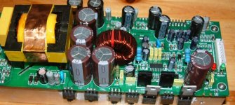
Pls find the schematic below,we have use this schematic in our 600W/4ohm amp .works well at 540KHZ and DT set as 45ns.
When we shorted the added diode ,the mosfet heat quickly ,we have to increase DT time (>100ns)to cool it .
But when we use this circuit ,it can works well at 540KHZ(osc frequency) and 45ns (DT time) and 600W(rated power <1%thd+n).
So we call it IRS2092 FAST AMP!
Simple way,Share with diyaudio member
We have use it in some type amp,bass well,sound intelligibility not good,how to improve this.
Maybe we will increase osc frequency,but when we increase it more than 500Khz we will meet mosfet heat loss increase and frequently protection or other problems.
Special schottky mosfet is easy way to make it reality,but high cost and no more choice are the most direct concern.
We have test many times ,at last we found one simple way to improve it performance and using common MOSFET.
1.COMMON MOSFET @ 540Khz
2.DT TIME @ 45ns
Pls find the schematic below,we have use this schematic in our 600W/4ohm amp .works well at 540KHZ and DT set as 45ns.
When we shorted the added diode ,the mosfet heat quickly ,we have to increase DT time (>100ns)to cool it .
But when we use this circuit ,it can works well at 540KHZ(osc frequency) and 45ns (DT time) and 600W(rated power <1%thd+n).
So we call it IRS2092 FAST AMP!
Simple way,Share with diyaudio member
Attachments
Last edited:
This is a classic approach often used with old and/or >200V MOSFET having high Qrr body diodes and not low enough Rds-on. Switching losses are reduced, but conduction losses increase.
Newer MOSFET up to 200V (like IRFB4227) can work "cool" without the diodes and without the dead time (I'm not sure whether this can be done with IRS2092).
Newer MOSFET up to 200V (like IRFB4227) can work "cool" without the diodes and without the dead time (I'm not sure whether this can be done with IRS2092).
We have test many times,Irfb4227 and 4229 will good performance in this topology.
the DT time can decrease 1/2 when in this circuit,I use irfb4227 at 600W board,dt set 75ns,the mosfet hot quickly,from normal to 90oc at rated power.but in this circuit,dt at 45 ns,same frequency,same condition,mosfet body tempreture only increase 20oc.
I suggest friends can discuss The diode choice .we use 40A ultrafast diode,
mosfet is irfb4227.
hi authxl
greetings is this schematic for diyers can you give part no of 40 ampere ultrafast
diode
thanking you
andrew lebon
Oh!
we parallel two 20A diode in the circuit.one thing maybe careful ,postive diode is schottky ,not ultralfast diode.if the current not enough ,you can parallel some.
Idea come from QSC PL380, Irfb4227 series schottky mosfet circuit suitable.
performance observably improved .
With IRFB4227 diodes are not needed at all, these MOSFET can work alone and free of body diode conduction up to 20A peak drain current, provided that proper gate drive timing is used. What I do with IR2110 may not be possible with IRS2092, as I pointed out early.
In other words, with these MOSFET only sub-optimal circuits will benefit from the diodes.
In other words, with these MOSFET only sub-optimal circuits will benefit from the diodes.
With IRFB4227 diodes are not needed at all, these MOSFET can work alone and free of body diode conduction up to 20A peak drain current, provided that proper gate drive timing is used. What I do with IR2110 may not be possible with IRS2092, as I pointed out early.
In other words, with these MOSFET only sub-optimal circuits will benefit from the diodes.
I suggest friends can try it or use data to prove useless or usful.
IRF4229 body diode 190ns,common ultral fast diode trr time 45ns,schocttky diode positive voltage 0.7V,no reverse time .
As engineer need try it and calculate than reason out a conclusion.
I try it once time just ago,my conclusion is right,very useful circuit.
I never try the irfb6648 or others,maybe will better.this conclusion is base on irfb4229 or irfb4227.
Driver engine is important indeed.
Attachments
Last edited:
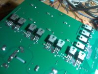
First picture: Full bridge with IRFB4227 pairs. No heatsink. Supply voltage reduced to 85V DC to cut losses (normally 170V).
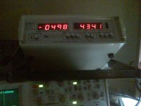
Second picture: 500W into 3.8 ohm according to Valhalla power meter.
I only pushed it to the point where keeping my finger on one of the pairs of IRFB4227 through a silicone pad started to become a bit uncomfortable. Current sharing is not optimal at all because there is no thermal tracking between pairs of MOSFET due to the lack of heatsink, so one pair tends to be hotter than the rest. I didn't want to push this prototype further, as I must ship it to my customer before 13:00 and I can't afford damaging it.
It does nearly full music output into 8 ohm and 4 ohm without heatsink.
No diodes used. They won't improve it. No dead time used either
Attachments
No dead time used either
just proper sized gate resistors which will do the job in this case
Hi all,
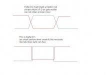
Is possible (in the case of large continuous power amplifiers) used a DT digital.
this is not difficult to obtain.
amplifiers in high-fidelity, cross-DT is to obtain the lowest distortion crossover (as class AB bias) , the amp will draw a certain current.
In the case I mentioned before, the "DT" did not cross and may have very little downtime or variables DT dynamically. (I prefer).
result is very good for powers higher than 2kW. (this need very fast pre-driver and driver stage with propagation times very small and very fast transient response)
In this case the gate of the MOSFET is driven directly (no rg + D).
regards
Last edited:
No dead time at all? Can you explain what is going on here?
Switching waveform does not "jump" when the amplifier goes from sourcing to sinking current and vice-versa. Timing is very tight, +/-10ns error only. The delay from PWM signal transition to switching node transition is determined by output current and is quite linear with respect to output current. This is achieved with the proper choice of ordinary parts (not matched or selected, but that would make it perform even better). No delay correction loops are used.
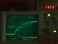
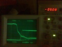
First picture: Gate and drain waveforms at 500W/4R sine. 10:1 probes. Lower MOSFET Vgs reaches turn-on plateau just when upper MOSFET Vds starts to rise.
Second picture: Gate and drain waveforms at 500W/4R sine. 10:1 probes. Same as above but for lower MOSFET turn-off. No ringing.
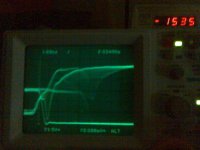
First picture: Gate and drain waveforms at 500W/4R sine. 10:1 probes. Same as first picture but at 1500W/4R. di/dt phase of turn-on process is clearly seen. di/dt is regulated to allow reliable use of body diodes with 2R loads (up to 40A per IRFB4227).
Attachments
Last edited:
...to die or not to die...
1. Already the definition of DT is depending on who you ask.
Some people, especially manufacturers of driver ICs, do use the term DT for the time when both driver outputs are below 10% of max.
Some other people do use the term DT without any definition.
I tend to define DT as the time when both Ugs (upper and lower MosFet) are below their threshold voltage. Means the time, when both switches are non conductive.
2. If you look to Ugs, to Uds and to Id - you will notice that there is no digital change between ON and OFF. It is an analogue transition, which typically takes place within a time frame of 5ns...100ns - depending on your choice of switching speed.
3. The transition details do massively depend on the situation. During idle you can achieve almost soft switching by fast transition towards OFF and getting benefit of parasitic capacitances, which define together with the ripple current a moderate dv/dt for Uds. Means you can reach almost ZVS.
At higher loads common half bridges and full bridges do show hard switching during many switching cycles. Here the properties of the body diodes (or external diodes) are crucial - and it is not just their trr, but more the Qrr! Please note: Qrr is depending on your choice for di/dt. Qrr is massively increasing with faster di/dt and also with temperature. Most often Qrr is specified at 100A/us and 25°C, but most class D amps are operating at di/dt between 300A/us and 1500A/us and junction temperatures between 50°C and 120°C....
4. You can adjust the switching timing even to a certain overlap. This is helpful to reduce distortion and if you optimize this overlap in combination with the ripple current of your filter, then this will cause just minor additional losses. But of course you must be able to ensure high switching precision. A deviation of 5 ns does already make a respectable difference. 50 ns are already pointing to the groove.
5. If you have to much overlap, then you will get a lot of heat and poor EMI.
(But theoretically you could avoid any current through the body diodes during all load conditions, when you adjust an overlap which causes during idle situation a shot peak of the same level which you are targeting at max output - by the expense of even worse and excessive shoot through losses instead of losses for removing Qrr... For sure such an extreme adjustment is not advisable ! )
)
6. If you have much to much overlap, then the power stage will burn pretty fast.
1. Already the definition of DT is depending on who you ask.
Some people, especially manufacturers of driver ICs, do use the term DT for the time when both driver outputs are below 10% of max.
Some other people do use the term DT without any definition.
I tend to define DT as the time when both Ugs (upper and lower MosFet) are below their threshold voltage. Means the time, when both switches are non conductive.
2. If you look to Ugs, to Uds and to Id - you will notice that there is no digital change between ON and OFF. It is an analogue transition, which typically takes place within a time frame of 5ns...100ns - depending on your choice of switching speed.
3. The transition details do massively depend on the situation. During idle you can achieve almost soft switching by fast transition towards OFF and getting benefit of parasitic capacitances, which define together with the ripple current a moderate dv/dt for Uds. Means you can reach almost ZVS.
At higher loads common half bridges and full bridges do show hard switching during many switching cycles. Here the properties of the body diodes (or external diodes) are crucial - and it is not just their trr, but more the Qrr! Please note: Qrr is depending on your choice for di/dt. Qrr is massively increasing with faster di/dt and also with temperature. Most often Qrr is specified at 100A/us and 25°C, but most class D amps are operating at di/dt between 300A/us and 1500A/us and junction temperatures between 50°C and 120°C....
4. You can adjust the switching timing even to a certain overlap. This is helpful to reduce distortion and if you optimize this overlap in combination with the ripple current of your filter, then this will cause just minor additional losses. But of course you must be able to ensure high switching precision. A deviation of 5 ns does already make a respectable difference. 50 ns are already pointing to the groove.
5. If you have to much overlap, then you will get a lot of heat and poor EMI.
(But theoretically you could avoid any current through the body diodes during all load conditions, when you adjust an overlap which causes during idle situation a shot peak of the same level which you are targeting at max output - by the expense of even worse and excessive shoot through losses instead of losses for removing Qrr... For sure such an extreme adjustment is not advisable !
)6. If you have much to much overlap, then the power stage will burn pretty fast.
signal is not clean, also up-side drivers not Have RC filter (constant) on bootstrapp. (it modulate)Switching waveform does not "jump" when the amplifier goes from sourcing to sinking current and vice-versa. Timing is very tight, +/-10ns error only. The delay from PWM signal transition to switching node transition is determined by output current and is quite linear with respect to output current. This is achieved with the proper choice of ordinary parts (not matched or selected, but that would make it perform even better). No delay correction loops are used.
First picture: Gate and drain waveforms at 500W/4R sine. 10:1 probes. Lower MOSFET Vgs reaches turn-on plateau just when upper MOSFET Vds starts to rise.
Second picture: Gate and drain waveforms at 500W/4R sine. 10:1 probes. Same as above but for lower MOSFET turn-off. No ringing.
First picture: Gate and drain waveforms at 500W/4R sine. 10:1 probes. Same as first picture but at 1500W/4R. di/dt phase of turn-on process is clearly seen. di/dt is regulated to allow reliable use of body diodes with 2R loads (up to 40A per IRFB4227).
perhaps the effects are positive, we can not evaluate these images only.
and then I see a lot of ripple on the power supply at ...only 500w?
- Status
- This old topic is closed. If you want to reopen this topic, contact a moderator using the "Report Post" button.
- Home
- Amplifiers
- Class D
- The simple way to improve the IRS2092 amp performance