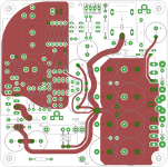
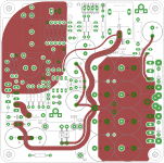
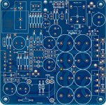
What is that brown area top left?
That's the area where I've made a mistake
 . The one single trace inside of the plane should have been part of that plane. Not that hard to fix but annoying anyway.
That plane is supposed to be the ground plane for the analog ground, which is connected to the main audio ground via a 1 ohm resistor. Single traces instead would probably have been possible, but I thought a plane (even a slotted one) doesn't cause any detrimental effects in this case. It's only carrying small signal currents.
Hi Preamp,
I am not a big expert in power amp PCB design but I have some doubts about your PCB design.
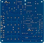
Why would not you make a solid ground pour for the PSU part similar to the signal ground pour and then connect them with 1 Ohm resistor or even a jumper since there going to be no high currents traveling through that connection. I also don't see why would you need to increase the power supply traces length by doing such a curly filter capacitors connections. Each sharp trace turn would radiate badly especially if you ask your amp to deliver max power (highest ripple currents situation). I guess a wide pour per rail covering all capacitors pins with a solid ground plane below would probably be better. Also, it is possible to make a CCRCC configuration for the PSU unit since you use four parallel caps per rail anyways. If you insert something like ~0.1 Ohm resistor between the first and the second filter capacitors pair for each rail it would remove some of the high frequency ripple harmonics. You can use radial (standing) type resistor from Ohmite or similar to place it between caps without taking much extra space.
Just my 2 ct.
Regards,
Oleg
I am not a big expert in power amp PCB design but I have some doubts about your PCB design.
Why would not you make a solid ground pour for the PSU part similar to the signal ground pour and then connect them with 1 Ohm resistor or even a jumper since there going to be no high currents traveling through that connection. I also don't see why would you need to increase the power supply traces length by doing such a curly filter capacitors connections. Each sharp trace turn would radiate badly especially if you ask your amp to deliver max power (highest ripple currents situation). I guess a wide pour per rail covering all capacitors pins with a solid ground plane below would probably be better. Also, it is possible to make a CCRCC configuration for the PSU unit since you use four parallel caps per rail anyways. If you insert something like ~0.1 Ohm resistor between the first and the second filter capacitors pair for each rail it would remove some of the high frequency ripple harmonics. You can use radial (standing) type resistor from Ohmite or similar to place it between caps without taking much extra space.
Just my 2 ct.
Regards,
Oleg
Hi Oleg,
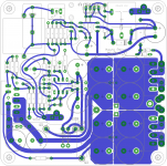
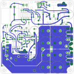
on the quick - something like this?
I'd actually doubt that there're any detrimental effects due to increased track length (they're not THAT long after all) or any sharp edges. I think that the 'vertical' edges where the PCB track changes into a capacitor lead would be much worse and swamp much anything that can be done with the copper pour.
OTOH track resistance will be minimized compared to the separately laid out tracks. But then again, they're more symmetrical to begin with and the tracks between the two capacitor banks act like a low value resistor, too.
Anybody willing to have both board versions made and test it out?
Attachments
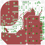
Hi Lasse,
It is better now. But you can do even better, IMO. Look here for an example of GND plane layout from ClaveFremen on his MyRef FE board. As you can see it covers all the supply traces and the output protection relay. Your concern is not only the trace resistance but also its parasitic inductance, therefore people are usually talking about impedance which includes both effects and is frequency dependent. What I learned from various discussions and designs on this forum is that one of the concerns in grounding is to make ground reference as stable as possible meaning near zero impedance. An infinite plane approaches this requirement the most. Assuming the GND potential is almost equal everywhere you can connect your output ground to this plane at any point. The long and relatively thin GND trace from the star ground point to the protection relay in your arrangement would have too high impedance to provide a reliable ground reference for the output. Same is true for the power rails ground layout. Make the power GND plane covering the supply traces all the way to the LM3886 power pins and make it as wide as you can within your layout.
I would also connect two grounds - power and signal - near the LM318 op-amp decoupling caps. This is where the supply for the op-amp goes and you want it to have low impedance too. At the same time there will be no high supply return currents passing through this connection since your power rails are routed away from this region. This way you can remove the resistor connecting the two grounds and just connect two GNDs together with a ~5 mm wide joint on the right side of LM318 outline. This is different from how MyRef FE board grounds are connected but I guess it is a better way of doing it. I recommend to consult this web page for a lot more information on the grounding of LM3886 amp from a professional. Tomchr does not give you a ready made layout but he gives a lot of information to make it right by yourself.
You have two diodes on the bottom of the PCB interfering with the resistor outline. I would rearrange these parts such that they do not overlap.
If you are not afraid of soldering big size SMD resistors I would recommend to replace standing resistors in the CCRCC configuration by the high wattage SMD type under the board. You can use two in parallel for each rail. I somehow overlooked initially how tight is the space between the capacitors.
Regards,
Oleg
Last edited:
What I learned from various discussions and designs on this forum is that one of the concerns in grounding is to make ground reference as stable as possible meaning near zero impedance. An infinite plane approaches this requirement the most. Assuming the GND potential is almost equal everywhere you can connect your output ground to this plane at any point.
That's right. But there is no such thing as an infinite plane! Best thing to do would be to use like a 5-layer board and use a whole layer for each of the supply lines, including ground, and make heavy use of buried vias. That's a little over the top here though, because the single- and double-layer boards made and used till this day seem to work just fine.
The long and relatively thin GND trace from the star ground point to the protection relay in your arrangement would have too high impedance to provide a reliable ground reference for the output.
I don't think so. Consider this trace to be a minor extension of the wire connecting the other end of the track with the speaker binding post, the actual speaker wire to the speaker itself, the speakers' binding post, the internal wiring to the crossover network... As long as that trace does not share its connection with anything else (and it doesn't) it's just that: an additional piece of speaker wire.
You have two diodes on the bottom of the PCB interfering with the resistor outline. I would rearrange these parts such that they do not overlap.
No problem here. The big resistors are to be raised at least 8mm from the PCB to allow for better air exchange, which leaves plenty of room for even the diodes to be raised a little. This way I don't have to sacrifice my neat and straight track runs
.I've had a brief look at the Fremen layout and decided that for me this was much too SMD-heavy, so I didn't explore it any further and stuck to Russ' previous layout work. It might not be perfect this way, but as long as it is doing fine, I'll be content.
This is your layout, so you are the King I just gave recommendations according to my understanding.
If just "doing fine" is sufficient then ordinary chipamp is much simpler and does just that - "doing fine" No need to go complicated route designing the PCB for a composite amp where the last bit of performance was the initial goal. All is IMHO
Regards,
Oleg
I just gave recommendations according to my understanding. It might not be perfect this way, but as long as it is doing fine, I'll be content.
If just "doing fine" is sufficient then ordinary chipamp is much simpler and does just that - "doing fine"
No need to go complicated route designing the PCB for a composite amp where the last bit of performance was the initial goal. All is IMHORegards,
Oleg
Naah, come on. The MyRef is a totally different animal than a GainClone, and certainly not because of the way the PCB is laid out .
Aside from that my layout is already at the board house, and since I'm not planning to do a second run for myself, any changes now are purely academic. Maybe you want do add your proposed refinements to my current layout and then post the gerbers here for future diy'ers?
.Aside from that my layout is already at the board house, and since I'm not planning to do a second run for myself, any changes now are purely academic. Maybe you want do add your proposed refinements to my current layout and then post the gerbers here for future diy'ers?
I already have MyRef FE and am happy with it. I like designing the PCBs but I'm more inclined towards SMD parts, so I would probably end up with the layout similar to MyRef FE
Good for you then, I guess
.I've read the excellent writeup from Tom you linked to and had a closer look at Fremen's layout now. As far as I have understood Tom, the FE layout is far from ideal though. It does indeed make use of a of a huge and low-impedance ground plane, but that alone does not make it a good grounding scheme. Tom proved with his simulations that there was a substantial improvement when he routed GND_SIG to GND_LOAD. If you have a look at the Fremen layout, however, you'll see that GND_SIG and GND_LOAD are as far away from each other as they can possibly be, both in terms of resistance and inductance. Since the ground pour is by no means "ideal" and still has some totally "real" resistance and inductance, the currents will follow the laws of physics and pick the path with least resistance or inductance. If you now superimpose those path on the ground plane, it will look pretty much like this: GND_SIG -- GND_PWR -- GND -- GND_LOAD, whereas the proposed best way would be: GND_SIG -- GND_LOAD -- GND_PWR -- GND.
Looking back at my layout then, it seems to be much more in accordance with Toms propositions. If I now run the 1R from the ground plane directly to the relay pin and not to the star ground, it should be pretty much spot on. You could argue about running the speaker return to the LM3886's caps first (which would be GND_PWR) and then back to the star ground (which wouldn't be a star by then anymore), but that indeed seems to be only increasing the track resistance/inductance without any real benefit. Maybe some thorough simulation is in order here
.Attachments
You do not have to argue with me I agree that there is no ideal layout as such. There are more or less good approximations of it. I also did not say that I agree with the power and signal GNDs connection on the MyRef FE PCB and I proposed my view on how to do it. With regards to GND planes/pours they do have their parasitics but to a much lesser degree than a thin trace. If I would redesign the MyRef PCB I would change the aspect ratio of the board and would move the entire power supply section to the left of the LM3886 as Tomchr did. This would allow to have shortest distance between power and output GNDs (which will be in the middle of the PCB) even if protection relay is used. Then the entire signal section would occupy the right side of the PCB and would make it easy to have a short undisturbed connection between signal and output GNDs. But this would probably be a distant copy of Tomchr's layout. In which case it is easier to get his excellent and fully tested boards and slip well ever after
I agree that there is no ideal layout as such. There are more or less good approximations of it. I also did not say that I agree with the power and signal GNDs connection on the MyRef FE PCB and I proposed my view on how to do it. With regards to GND planes/pours they do have their parasitics but to a much lesser degree than a thin trace. If I would redesign the MyRef PCB I would change the aspect ratio of the board and would move the entire power supply section to the left of the LM3886 as Tomchr did. This would allow to have shortest distance between power and output GNDs (which will be in the middle of the PCB) even if protection relay is used. Then the entire signal section would occupy the right side of the PCB and would make it easy to have a short undisturbed connection between signal and output GNDs. But this would probably be a distant copy of Tomchr's layout. In which case it is easier to get his excellent and fully tested boards and slip well ever afterYou do not have to argue with me
I don't
. Just wanted to point out that even the Fremen layout might have some room for improvements.(And to stop other readers from bashing my layout and building a FE instead, of course
)But this would probably be a distant copy of Tomchr's layout. In which case it is easier to get his excellent and fully tested boards and slip well ever after
Where's the fun in that?
And Tom doesn't sell boards for the MyRef, does he?
And Tom doesn't sell boards for the MyRef, does he?
No, he does not. But his boards, although lacking the DC protection and full power section on board, are still incredibly good. It does not always have to be the MyRef monoblock design to be good
It does not always have to be the MyRef monoblock design to be good
That's undeniable. But at the moment it's the MyRef that I want to give a try. Maybe I'll get myself some of Tom's boards if the MyRef doesn't knock me over.


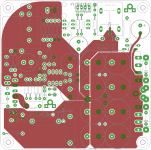
Hi Lasse,
This looks better but still can be improved, IMO.
Why wouldn't you skip the star ground idea and make a solid GND plane for the power and output section? As it is done now, you force all the pulsating return currents through a tiny spot which has increased impedance. As a result your reference ground point will "dance" with the output signal due to alternating positive and negative return currents going through this tiny spot and generating error potential.
Another point of concern is the connection point between the power and signal grounds. Just try to draw on your PCB the supply current flow for the LM318. Start from its supply bypass capacitors and follow it through the output of the LM318 to the LM3886 and back via ground connection to the ground pins of the same bypass caps where you started. Does the forward current follow the return current with the smallest possible loop area? On the MyRef FE PCB there is only one supply bypass cap from rail to rail which somehow remedy this. I guess the idea behind is that LM318 works in a sort of single polarity supply (from V- to V+) mode and "knows" nothing about the existence of the ground potential. But I guess it is not totally true since the signal is ground referenced and the supply to the LM318 is bipolar thus three bypass caps are probably fine but you should provide an appropriate ground return for the supply currents. I would recommend to connect power and signal grounds under the LM318 supply bypass capacitors without using the 1 Ohm resistor.
All my suggestions are according to my limited understanding, so not necessarily correct May be someone more experienced can correct me if I'm wrong.
Regards,
Oleg
This looks better but still can be improved, IMO.
Why wouldn't you skip the star ground idea and make a solid GND plane for the power and output section? As it is done now, you force all the pulsating return currents through a tiny spot which has increased impedance. As a result your reference ground point will "dance" with the output signal due to alternating positive and negative return currents going through this tiny spot and generating error potential.
Another point of concern is the connection point between the power and signal grounds. Just try to draw on your PCB the supply current flow for the LM318. Start from its supply bypass capacitors and follow it through the output of the LM318 to the LM3886 and back via ground connection to the ground pins of the same bypass caps where you started. Does the forward current follow the return current with the smallest possible loop area? On the MyRef FE PCB there is only one supply bypass cap from rail to rail which somehow remedy this. I guess the idea behind is that LM318 works in a sort of single polarity supply (from V- to V+) mode and "knows" nothing about the existence of the ground potential. But I guess it is not totally true since the signal is ground referenced and the supply to the LM318 is bipolar thus three bypass caps are probably fine but you should provide an appropriate ground return for the supply currents. I would recommend to connect power and signal grounds under the LM318 supply bypass capacitors without using the 1 Ohm resistor.
All my suggestions are according to my limited understanding, so not necessarily correct
May be someone more experienced can correct me if I'm wrong.Regards,
Oleg
Last edited:
Why wouldn't you skip the star ground idea and make a solid GND plane for the power and output section?
To keep the large current spikes from the 'lytics separated from the signal ground. In my opinion this will work out much better to keep the signal ground from 'dancing' on the rectifier current spikes. Or to put it another way: If the capacitor banks were on a separate PCB, that millimeter of track to the star ground would be the equivalent of a wire running from the cap PCB to the amp PCB.
Another point of concern is the connection point between the power and signal grounds. Just try to draw on your PCB the supply current flow for the LM318.
Will do that the next days.
That 1R resistor is included in the original schematic from Mauro btw.; I guess he knew why he put it there
.I consider this current route analysis very important.....................................Just try to draw on your PCB the supply current flow for the LM318. Start from its supply bypass capacitors and follow it through the output of the LM318 to the LM3886 and back via ground connection to the ground pins of the same bypass caps where you started. Does the forward current follow the return current with the smallest possible loop area? ..................
You must reduce loop area for the flow and return currents to pass from any source. You must do this for EVERY source that supplies some current.
I'm having a hard time figuring out where the output current of the LM318 actually goes to . This, in turn, would lead me to the conclusion that another ground plane, connected at one point to the power and output ground (probably under the LM318 supply bypass capacitors), would be the "most appropriate" solution. But this somehow seems to contradict the simulation results published by Tom, which clearly show a benefit from connecting the input signal ground to the output ground first. Can't get my head around this .
On one hand it seems like a waste of money to start a second board run now and build two prototypes on two different boards, and later toss the worse one. On the other hand, this is probably the only way to find out for sure... which is absolutely to my liking, after all!
What shall I do now?
The most logical thing to do would be to populate one of the boards that arrived today [man, that was fast, not even two weeks!] and measure it up. If the performance is top notch already, I can surely stand to not know how much better it might become .
. This, in turn, would lead me to the conclusion that another ground plane, connected at one point to the power and output ground (probably under the LM318 supply bypass capacitors), would be the "most appropriate" solution. But this somehow seems to contradict the simulation results published by Tom, which clearly show a benefit from connecting the input signal ground to the output ground first. Can't get my head around this .On one hand it seems like a waste of money to start a second board run now and build two prototypes on two different boards, and later toss the worse one. On the other hand, this is probably the only way to find out for sure... which is absolutely to my liking, after all
!What shall I do now?
The most logical thing to do would be to populate one of the boards that arrived today [man, that was fast
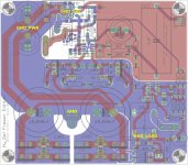
, not even two weeks!] and measure it up. If the performance is top notch already, I can surely stand to not know how much better it might become .What about this? Still a bit "starry", but it doesn't immediately mix signal ground with output ground. Where should one draw the line between maximising ground pour and separating or "linking" the different ground points?
[flatbed scanner makes for a good PCB camera. Seems like I screwed up one more time and forgot the part's values on the silk screen...]
[flatbed scanner makes for a good PCB camera
. Seems like I screwed up one more time and forgot the part's values on the silk screen...]Attachments
- Status
- This old topic is closed. If you want to reopen this topic, contact a moderator using the "Report Post" button.
- Home
- Amplifiers
- Chip Amps
- My new monobloc layout for Mauro Penasa's MyRef Rev. C