Hello everybody. It was a long time I had some TPA6120A2 chips to test and finally I put all together.. My headphone amplifier project is based on some ideas from other similar projects, mainly peranders and Daki][er.
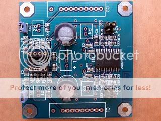
Here is how looks like:
There is a voltage regulator section, with an LM317 and an LM337 for positive and negative rails. I put two 10 turns trimmers to regulate exactly the same positive and negative voltages.
The audio section includes a Panasonic EVJ series input stereo potentiometer, followed by two 10 uF WIMA Polyester capacitors and a first buffer. From simulation, the input buffer should have an almost flat response from 2 Hz up to around 100 kHz. This has been confirmed also from some measurements on the prototype.
Input buffer response (from simulation):
After this buffer there is the king of the project, the TPA6120.
Both the buffer and the TPA are powered at +/- 12V, but the voltage can be changed using the trimmers from +/- 6V to +/- 15V.
The input buffer (a dual opamp) is on a socket and this allows to test different solutions without any desoldering.
Here is the schematic:
and this is the board:
The board is single layer and this allowed me to easily make it at home (using toner transfer method). On the back of the PCB there are some "manual" connections of the + and - rails and some GNDs. All the signal nets are on the top of the PCB. Only the 2 feedbacks of the TPA are in the bottom, connected manually (see below picture), but no signs of oscillation has been observed.
This is another picture of the whole board:
On the input buffer there are a couple of 10 uF cerafine and 0,1 uF PPS capacitors on the power supplies. For the TPA the energy reserve is given by a couple of 0,1 PPS and 47 uF low esr tantalium. Other SMD capacitors on the audio path are C0G or NP0.
But how it sounds?
AWESOME! As input buffer I tested it with the OPA2134, the AD826 and the AD8620. I must say that the sound with every of these opamps is a little different.
The OPA2134 gives a typical Burr-Brown sound, warm and smooth.. I'm a little bored of this kind of sound, so I tested other alternatives.
The AD826 gives a sound much more sharp and definite. Like cleaning the crystal of a glass.. you see through what is inside")
I tested also the AD8620 (on ad soic-dip adapter), and the sound is similar to the AD826. Maybe also a little more clear and accurate, so I left this opamp. By the way, this was also the choice of peranders and Daki][er.. probably they made my same tests..
On the output the offset is around 6-8 mV, safe for any headphone.
This chip is really good and capable of great power. it drives without any effort my HD650.
Finally I tested the ampli attached to my USB soundcard (based on PCM2906 + OPA2353).
The TPA makes a miracle also in this case. I chosen the OPA2353 for an USB-powered project because it's rail to rail and works with the USB port 5V but has some output power limitations. While other headphones sound fine with the OPA2353, the Sennheiser HD650 is a little too hard... the TPA6120 after it brings a complete new life to the sound!
Here is how looks like:
An externally hosted image should be here but it was not working when we last tested it.
There is a voltage regulator section, with an LM317 and an LM337 for positive and negative rails. I put two 10 turns trimmers to regulate exactly the same positive and negative voltages.
The audio section includes a Panasonic EVJ series input stereo potentiometer, followed by two 10 uF WIMA Polyester capacitors and a first buffer. From simulation, the input buffer should have an almost flat response from 2 Hz up to around 100 kHz. This has been confirmed also from some measurements on the prototype.
Input buffer response (from simulation):
An externally hosted image should be here but it was not working when we last tested it.
After this buffer there is the king of the project, the TPA6120.
Both the buffer and the TPA are powered at +/- 12V, but the voltage can be changed using the trimmers from +/- 6V to +/- 15V.
The input buffer (a dual opamp) is on a socket and this allows to test different solutions without any desoldering.
Here is the schematic:
An externally hosted image should be here but it was not working when we last tested it.
and this is the board:
An externally hosted image should be here but it was not working when we last tested it.
The board is single layer and this allowed me to easily make it at home (using toner transfer method). On the back of the PCB there are some "manual" connections of the + and - rails and some GNDs. All the signal nets are on the top of the PCB. Only the 2 feedbacks of the TPA are in the bottom, connected manually (see below picture), but no signs of oscillation has been observed.
An externally hosted image should be here but it was not working when we last tested it.
This is another picture of the whole board:
An externally hosted image should be here but it was not working when we last tested it.
On the input buffer there are a couple of 10 uF cerafine and 0,1 uF PPS capacitors on the power supplies. For the TPA the energy reserve is given by a couple of 0,1 PPS and 47 uF low esr tantalium. Other SMD capacitors on the audio path are C0G or NP0.
But how it sounds?
AWESOME! As input buffer I tested it with the OPA2134, the AD826 and the AD8620. I must say that the sound with every of these opamps is a little different.
The OPA2134 gives a typical Burr-Brown sound, warm and smooth.. I'm a little bored of this kind of sound, so I tested other alternatives.
The AD826 gives a sound much more sharp and definite. Like cleaning the crystal of a glass.. you see through what is inside
I tested also the AD8620 (on ad soic-dip adapter), and the sound is similar to the AD826. Maybe also a little more clear and accurate, so I left this opamp. By the way, this was also the choice of peranders and Daki][er.. probably they made my same tests..
On the output the offset is around 6-8 mV, safe for any headphone.
This chip is really good and capable of great power. it drives without any effort my HD650.
Finally I tested the ampli attached to my USB soundcard (based on PCM2906 + OPA2353).
An externally hosted image should be here but it was not working when we last tested it.
The TPA makes a miracle also in this case. I chosen the OPA2353 for an USB-powered project because it's rail to rail and works with the USB port 5V but has some output power limitations. While other headphones sound fine with the OPA2353, the Sennheiser HD650 is a little too hard... the TPA6120 after it brings a complete new life to the sound!

 Congratulations,you also like the TPA6120? This is my favorite at the moment.
The design is very similar as mine.
Some comments:
I'll believe you haven't soldered the PowerPad? How about cooling?
RA why? I think R5 is enoug.
C9, way too small. I have 1 nF instead of 10 pF. With volume at half you have 25k source impedance and the filter frequency should be 100-200 kHz. 100-1000 pF seems more appropiate.
C15 is not very useful, doesn't harm either. With gain of 2.8 this cap will have very little influence on stability. This cap is useful with both source impedance and feedback has rather high values. Then the input capacitance of the opamp will create instability so this cap is to cancel out this input capacitance. This is the real important purpose but then you can also have to tailoring the frequency properties.
To trim the voltage isn't particulary necessary as long as they are rather equal. The reliability of pot is always worse than a plain resistor. An another rule of thomb is tonever connect only two terminal of a pot. Better to use all three in case of failure.
Thanks Netlist, digi01 and peranders! Actually this was my first serious headamp project and I'm pretty happy with it!
Some comments to peranders suggestions:
Yep.. I made some ridiculous attempts to make some little holes under the powerpad and tried to blow inside some tin with hot air , but realized that this was impossible. So I used a different philosophy: I spreaded a subtle layer of tin on the PCB side under the powerpad and also on the powerpad itself, then soldered all the other pins of the chip, while pressing the TPA against the PCB. I don't think that the pad has been soldered but for sure it has a good physical contact.
When it is working, the TPA is just a little warm.. I can keep my finger on it, so this point is ok (this was one of my concerns about this project).
You are right.
Actually I made many simulations of the input section before selecting these values...
With 1000 pF the input filter begins to cut around 10-20 kHz and the phase is already at -60 deg at 100 kHz.
I'd like to make it flat until 100 kHz to have the possibility to use it also as pre-amplifier for audio measurements done at sample rate of 192 kHz.
Yes, it's too low for influencing stability. I've chosen this value again after simulations to make the cut-off response a little smoother.
Well, the real reason for the trimmers is that in this way I can change the +/- voltage as I like, so I can adapt the circuit to different power sources or test an input opamp that requires lower or higher power supply. Now I keep at +/-12V but can be adjusted from +/-6V to +/-15V.
Some comments to peranders suggestions:
peranders said:
I'll believe you haven't soldered the PowerPad? How about cooling?
Yep.. I made some ridiculous attempts to make some little holes under the powerpad and tried to blow inside some tin with hot air
, but realized that this was impossible. So I used a different philosophy: I spreaded a subtle layer of tin on the PCB side under the powerpad and also on the powerpad itself, then soldered all the other pins of the chip, while pressing the TPA against the PCB. I don't think that the pad has been soldered but for sure it has a good physical contact. When it is working, the TPA is just a little warm.. I can keep my finger on it, so this point is ok (this was one of my concerns about this project).
peranders said:RA why? I think R5 is enoug.
[/B]
You are right.
peranders said:C9, way too small. I have 1 nF instead of 10 pF. With volume at half you have 25k source impedance and the filter frequency should be 100-200 kHz. 100-1000 pF seems more appropiate.
[/B]
Actually I made many simulations of the input section before selecting these values...
With 1000 pF the input filter begins to cut around 10-20 kHz and the phase is already at -60 deg at 100 kHz.
I'd like to make it flat until 100 kHz to have the possibility to use it also as pre-amplifier for audio measurements done at sample rate of 192 kHz.
peranders said:C15 is not very useful, doesn't harm either. With gain of 2.8 this cap will have very little influence on stability. This cap is useful with both source impedance and feedback has rather high values. Then the input capacitance of the opamp will create instability so this cap is to cancel out this input capacitance. This is the real important purpose but then you can also have to tailoring the frequency properties.
[/B]
Yes, it's too low for influencing stability. I've chosen this value again after simulations to make the cut-off response a little smoother.
peranders said:To trim the voltage isn't particulary necessary as long as they are rather equal. The reliability of pot is always worse than a plain resistor. An another rule of thomb is to never connect only two terminal of a pot. Better to use all three in case of failure. [/B]
Well, the real reason for the trimmers is that in this way I can change the +/- voltage as I like, so I can adapt the circuit to different power sources or test an input opamp that requires lower or higher power supply. Now I keep at +/-12V but can be adjusted from +/-6V to +/-15V.
I must correct myself a bit. The C9 with 50 k volume pot and 100-200 kHz cut off should be 33-68 pF.
If you want to change the voltage to pot should be between ADJ and ground. I this way you will have a constant current through the feedback so the working conditions will be the same with different voltages.
If you want to change the voltage to pot should be between ADJ and ground. I this way you will have a constant current through the feedback so the working conditions will be the same with different voltages.
peranders said:I must correct myself a bit. The C9 with 50 k volume pot and 100-200 kHz cut off should be 33-68 pF.
If you want to change the voltage to pot should be between ADJ and ground. I this way you will have a constant current through the feedback so the working conditions will be the same with different voltages.
Thank you for the suggestions peranders.
For the power supply, I'm now using the ampli powered from a small switching smps designed around an LM2596 (with a double inductor for obtaining the 2 voltage rails from a single supply), and I must say that it sounds also better than using a normal linear power supply. Maybe it's just an impression.. but I have no idea on how to measure the difference of behavior at the sound output side, except my ears obviously.
In next release I'll try to merge them on the same PCB..
bye,
Paolo
peranders said:Have you had any opportunity to do anything about your project?
no.. due to lack of time. More urgent jobs pending
But, since I built it, I listened to it every day and I'm very satisfied! And I verified that also the cooling of the TPA is ok on the long period.
I'm using it now powered by this small smps:
An externally hosted image should be here but it was not working when we last tested it.
An externally hosted image should be here but it was not working when we last tested it.
so I can use a single supply, since the smps has a dual output (obtained with a dual inductor). And it seems that the TPA project sounds better with the smps than using a normal linear dual power supply. So my next step will be a more compact design of a single PCB with the LM2596 and the TPA.
I seriously doubt that because making a really quiet SMPS is not something you just like that. I'll imagine you have no control over the emission but nevertheless it's fun to explore the possibilities.paologatto said:And it seems that the TPA project sounds better with the smps than using a normal linear dual power supply. So my next step will be a more compact design of a single PCB with the LM2596 and the TPA.
Just wondering: When you have so low power consumption, why using a SMPS?
If you anyway want to integrate the PS, why don't you make it SMD as much as possible? Small and tight is good in most cases.
well, actually the smps that you see in the picture is at 4' or 5' release.. I designed and redesigned it (trial and error ) until this one. The re-design was to obtain the most quiet possible, for audio use (I used it with a DAC based on PCM1704, an ADC with PCM1804 and now with the TPA). On the output and on the input I have a residual ripple < 1mV, and this is good for an smps.
I verified also with an FFT oscilloscope and an EM probe that the emitted noise is low. Probably it could pass also a CE certification.
This is the simple schematic of the smps (here it has also +/- 5V):
The total consumption of the smps + TPA amplifier is 4,2 W.
The only smps takes 1,4 W with no load.
All this can be made better removing the redundant regulators.
You are right about using SMD.. I made these 2 using the components that I had in house, but I have already a list of SMD components to purchase for next release..
With all SMD components maybe that also an USB input with PCM2906 could be added.
Space: 100x80 mm = what my light license of Eagle allows me to manage.. but this is an additional challenge that I like!
) until this one. The re-design was to obtain the most quiet possible, for audio use (I used it with a DAC based on PCM1704, an ADC with PCM1804 and now with the TPA). On the output and on the input I have a residual ripple < 1mV, and this is good for an smps. I verified also with an FFT oscilloscope and an EM probe that the emitted noise is low. Probably it could pass also a CE certification.
This is the simple schematic of the smps (here it has also +/- 5V):
An externally hosted image should be here but it was not working when we last tested it.
The total consumption of the smps + TPA amplifier is 4,2 W.
The only smps takes 1,4 W with no load.
All this can be made better removing the redundant regulators.
You are right about using SMD.. I made these 2 using the components that I had in house, but I have already a list of SMD components to purchase for next release..
With all SMD components maybe that also an USB input with PCM2906 could be added.
Space: 100x80 mm = what my light license of Eagle allows me to manage.. but this is an additional challenge that I like!

 Is it a buffer + a non-inverting amp?
- Status
- This old topic is closed. If you want to reopen this topic, contact a moderator using the "Report Post" button.
- Home
- Amplifiers
- Chip Amps
- Yet another TPA6120A2 Headamp project