Hi everybody , I just dug up some info that might help to understand the innards of the TDA7293.
It´s datasheet provides very limited info on this chip but comparing the data-sheets of the various versions I noticed that the one for the TDA7294 does show a block-diagram of the chips innards . It is basic and does not go into much detail but I think it can help to understand the possible use of the 7293´s output buffer in a circuit driven by a separate op-amp and VAS-stage . Check it out if you please. Thanks M.
It´s datasheet provides very limited info on this chip but comparing the data-sheets of the various versions I noticed that the one for the TDA7294 does show a block-diagram of the chips innards . It is basic and does not go into much detail but I think it can help to understand the possible use of the 7293´s output buffer in a circuit driven by a separate op-amp and VAS-stage . Check it out if you please. Thanks M.
It will be interesting an amplifier made with separate op-amp and VAS-stage and two-three TDA7293 parallels output stages and a G-class power supply.
I made years ago an amplifier with 2 output stages and a G-class power supply and was interesting but I wanted more speed (8.4V/µsec was too slow for me) and I preferred full transistors amplifiers.
The questions is if is not become too complicated an amplifier like this.
I made years ago an amplifier with 2 output stages and a G-class power supply and was interesting but I wanted more speed (8.4V/µsec was too slow for me) and I preferred full transistors amplifiers.
The questions is if is not become too complicated an amplifier like this.
A few years ago I built a similar inverting TDA7293 with separate ±VSS and ±PWVSS as +VSS = +PWVSS +10V and -VSS=-PWVSS -10V. In this way you don't need bootstrap cap. BTL configuration (slew rate around 20V/us) worked nice.
I don't think that any circuit would increase the slew rate except BTL configuration.
On the other hand, applying too much corrections in the feedback might diminish further the slew rate in a composite circuit, which would be really bad.
I don't think that any circuit would increase the slew rate except BTL configuration.
On the other hand, applying too much corrections in the feedback might diminish further the slew rate in a composite circuit, which would be really bad.
Hello WLA what you have done seems to be a very different thing from what is being done here.
Of course nothing will increase the slew rate as long as the input-circuitry of the TDA is involved in anything but if the TDA is used in a composite amp it is the op-amp and its precision and low noise figure that become dominant as the TDA becomes "a tool" of said op-amp which is a lot faster and more precise . Plus you do not apply any more corrections in the ffedback at all since both the op-amp and the TDA are within the same feedback-loop.
On the other hand if we can use the op-amp followed by a fast VAS-stage and we only use the output buffer of the TDA ( the complete input and voltage amplification of the TDA are not used anymore ) then the only limitation of the slew-rate of the whole circuit is due to the output-buffer from the TDA which is probably higher than the rest of it , and the used op-amp so it could be a lot faster than the TDA itself . There are indications that the slew-rate of the TDA is limited by the ability of its internal current-source and sink driving the output-buffer ( pin 11 of the chip )
The TDA has a mosfet-power-output- buffer ! so if interestas resd the following link :
CordellAudio.com - Why I Prefer Power MOSFETs
Cheers Michael
Last edited:
Yes that is the idea . I only want to use the output buffer of one or more TDA7293 , as they provide a complete output-stage with protection circuitry , and use a good op-amp as input and feedback stage , and a fast voltage-amplifier in between both , and then see what I get . In any case it would /will be a hybrid between a discreete amp and a chip-amp but combining the advantages of both worlds . That is more or less what my idea boils down to.
Imagine an op-amp , three transistors , 1xBC560 and a pair of BF469/BF470 , and three TDA , on a PCB of 100x50mm , Enough to drive a good subwoofer or a large 3-way box ......as with 3 of them in parallel one can use 48volt rails
Imagine an op-amp , three transistors , 1xBC560 and a pair of BF469/BF470 , and three TDA , on a PCB of 100x50mm , Enough to drive a good subwoofer or a large 3-way box ......as with 3 of them in parallel one can use 48volt rails
Last edited:
it appears you can use an external VAS to operate the output stage via pin 11 if it is in the correct mode. no idea what the drive load is.
It may be better to use pin 11 as a comp pin to make it stable at a gain of 2 as well as use a separate regulated supply for the VAS stage.
It should be very easy to place 2SC5200,2SA1943's on the power pins to increase output current.
It may be better to use pin 11 as a comp pin to make it stable at a gain of 2 as well as use a separate regulated supply for the VAS stage.
It should be very easy to place 2SC5200,2SA1943's on the power pins to increase output current.
Last edited:
Got them from China but I know how to measure them to know if they are the real thing , tested them already. They cannot fake laser-engraving and more important they cannot fake several resistance-measurements between pins of the original ones !
At a 1.50 each if they were fakes I can still use them for other means and experiments
At a 1.50 each if they were fakes I can still use them for other means and experiments
Last edited:
Of the tda7293 there are several versions which has been discussed here. I believe they are V6 and v7 mainly. Can't remember which is which but one can take a higher voltage.
That said, if you want an amp that works with both, 4 and 8 ohms I wouldn't even go up to +-35v.
I tested mine with 4 ohms and 2x22vac and the temperature protection kicked in before 1minute passed. That was with full swing and sinewaves though. You will need a good thermal coupling to a big heatsink if you want to use +-35v with 4ohms. I personally would go with the values from the lm3886's datasheet and stick with +-28v or so for 4 ohms (~18vac).
Can you show me the circuit?A few years ago I built a similar inverting TDA7293 with separate ±VSS and ±PWVSS as +VSS = +PWVSS +10V and -VSS=-PWVSS -10V. In this way you don't need bootstrap cap. BTL configuration (slew rate around 20V/us) worked nice.
I don't think that any circuit would increase the slew rate except BTL configuration.
On the other hand, applying too much corrections in the feedback might diminish further the slew rate in a composite circuit, which would be really bad.
TDA7293 on V6 can handle up to 40v rail , V7 can take 50V rail.Of the tda7293 there are several versions which has been discussed here. I believe they are V6 and v7 mainly. Can't remember which is which but one can take a higher voltage.
That said, if you want an amp that works with both, 4 and 8 ohms I wouldn't even go up to +-35v.
I tested mine with 4 ohms and 2x22vac and the temperature protection kicked in before 1minute passed. That was with full swing and sinewaves though. You will need a good thermal coupling to a big heatsink if you want to use +-35v with 4ohms. I personally would go with the values from the lm3886's datasheet and stick with +-28v or so for 4 ohms (~18vac).
Provide Big heatsink and 35V rail , everything will be fine.
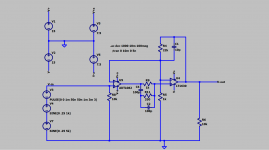
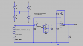
I am still working on my circuit and do not know what WLA was working on , but anyway here goes . Just take a good op-amp input-stage using LM 49720 for example , followed by a long tail pair of BC560 with an emitter-degeneration and a current-mirror , about 220 ohm-resistors , to transfer the op-amps output to the negative railvoltage , then follow that with a complementary VAS-stage using any good pair of complementary transistors with 100V max , a gain of 50 or higher , like BF469/BF470 see datasheet , where the upper transistor is configured as a constant current source set to about 10...15mA , and inject the output into the pin 11 of a slave-configured TDA7293. Experiment along these lines , you can , if you want , take the vas of a well known and well performing discreete amp and copy it . Feedback from output of TDA to inverting input of the opamp . The closed loop gain can be unit provided the vas is compensated for high frequency so you atre not limited by the gain of the TDA , normally 20x minimum. this is aprox what I am working on.
What I am trying out now is a second feedback from the output of the vas to the long-tailed pair to linearize these two stages to the max. Then the over-all feedback , due to the extremely high open loop gain of the op-amp, should get me vanishingly low distortion as long as the TDA´s output-buffer functions correctly with rising frequency so it will help me to find out what the frequency-bandwith of this buffer without the rest of the TDA is , because both the op-amp and the vas will not be the limiting factor .
What I am trying out now is a second feedback from the output of the vas to the long-tailed pair to linearize these two stages to the max. Then the over-all feedback , due to the extremely high open loop gain of the op-amp, should get me vanishingly low distortion as long as the TDA´s output-buffer functions correctly with rising frequency so it will help me to find out what the frequency-bandwith of this buffer without the rest of the TDA is , because both the op-amp and the vas will not be the limiting factor .
Last edited:
Hello Mike,
do you have news for us? Do your circuit work as expected?
Otherwise here is some news from me, another circuit topology that does fine in simulation and needs a prototype to see if this works also in reality. This time i had an eye especially on the risetime of the ICs envolved. (Again this are only ICs that are similar in characteristic to the ones to get used in the real circuit!)
Attachments
- Home
- Amplifiers
- Chip Amps
- TDA 7293 -- done right ?