I had a look for an actual high quality soundcard - and this one is one i would like to test:
Tascam US-1x2HR
the only thing i miss is a digital SPDIF- output which is very helpful when measuring loudspeakers by using DSP loudspeaker crossovers like the miniDSP 4x10 or the behringer DCX2496 for example
Tascam US-1x2HR
the only thing i miss is a digital SPDIF- output which is very helpful when measuring loudspeakers by using DSP loudspeaker crossovers like the miniDSP 4x10 or the behringer DCX2496 for example
I think it might well work with the tda almost as is , that is MODIFYING the pcb for the connections and the different small feedback caps to adapt it to the characteristics of the tda , and of course change the elecrolytics for the higher voltage. Question is :
COULD IT BE TRUE ?
I am considering sending the gerbers to JLCPCB to order a few boards then play around with them adding the TDA on the fly , feedback resistor directly on the pins of the chip.
The circuit reminds me of the old QUAD 405 as that was a current pump
COULD IT BE TRUE ?
I am considering sending the gerbers to JLCPCB to order a few boards then play around with them adding the TDA on the fly , feedback resistor directly on the pins of the chip.
The circuit reminds me of the old QUAD 405 as that was a current pump
Last edited:
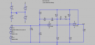
my variation of the my_ref-circuit
here is my variation of the my-ref-circuit you have linked, MalleMike.
it shows more a promising result to me than the original circuit in the link - at least in simulation... so this were the curcuit to test for me!
here is my variation of the my-ref-circuit you have linked, MalleMike.
it shows more a promising result to me than the original circuit in the link - at least in simulation... so this were the curcuit to test for me!
Attachments
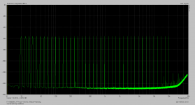
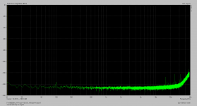
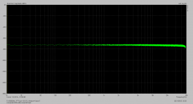
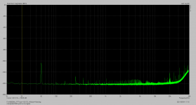
here are some measurements for my composite NFB design, the first thing that I show is the test of the soundcard quality:
terratec phase X24FW, used sample rate 96kHz, resolution 24bit
Attachment 1:
soundcard loop with white noise to see the soundcrds bandwidth - it is 48kHz (souncard has the same bandwidth when using 192kHz sample rate, so this is the hardware limit)
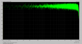
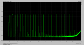
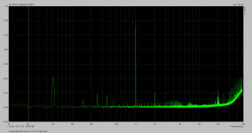
Attachment 2:
soundcard loop with no signal to see the cards noise
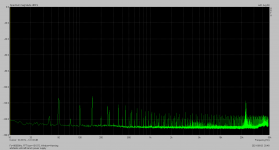
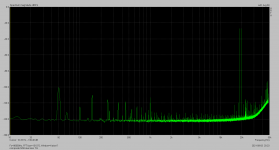
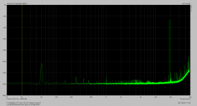
Attachment 3:
soundcard loop with 1kHz testtone to see the soundcards response to this signal
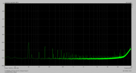
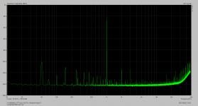
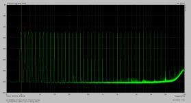
Attachment 4:
soundcard loop with a dual sine testtone 19kHz and 20kHz (1:1) to see if the soundcard shows intermodulation artefakte
Attachment 5:
soundcard loop with multitone testsignal to see the soundcards answer to this signal
as the soundcard has symmetrical quarter inch connectors the loop was done symmetrical
conclusion so far: this soundcard can be used for testing the amplifier
terratec phase X24FW, used sample rate 96kHz, resolution 24bit
Attachment 1:
soundcard loop with white noise to see the soundcrds bandwidth - it is 48kHz (souncard has the same bandwidth when using 192kHz sample rate, so this is the hardware limit)
Attachment 2:
soundcard loop with no signal to see the cards noise
Attachment 3:
soundcard loop with 1kHz testtone to see the soundcards response to this signal
Attachment 4:
soundcard loop with a dual sine testtone 19kHz and 20kHz (1:1) to see if the soundcard shows intermodulation artefakte
Attachment 5:
soundcard loop with multitone testsignal to see the soundcards answer to this signal
as the soundcard has symmetrical quarter inch connectors the loop was done symmetrical
conclusion so far: this soundcard can be used for testing the amplifier
Attachments
power supply artefakte
the power supply used to test the amplifier was a fourty year old regulated bench power supply (2x30V, 2x2,5A), connected to the supply 2x20mF and the amplifier, the shown signals are taken from the amps output.
Attachment 1:
power supply artefakte with the amps input shorted
Attachment 2:
power supply and measurement loop artefakte, loop connection is single ended, no signal is applied
conclusion so far:
a switched mode power supply will put the supplys artefakte out of the audible band and a symmetrical signal connection will avoid groundloops
Attachments
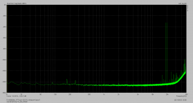
amplifier test with 8 Ohm resistive load, 1W
here are some measurements of the amplifier, just mounted on a heatsink, no further surrounding
Attachment 1:
1kHz testtone, one can see the typical k2 and k3 fingerprint of the TDA
Attachment 2:
19kHz and 20kHz dual sine testtone, one can see some intermodulation artefakte well below the signal
Attachment 3:
multitone test signal, a signal that comes close to real music in my eyes, the only thing disturbing is the power supplys artefakte
Attachment 4:
white noise bandwidth test, one can see that the bandwidth is the same as for the soundcard loop test, so the soundcard is the limiting element, as the 1W bandwidth measured with tone-generator and oscilloscope is 350kHz
conclusion so far:
mesurements look good to me, but i did not expect to see the TDAs "fingerprint"
Attachments
This does look very good and especially for a first test run . ")
The power-supply is a smps type with two very large filter-caps which are not good at veryhigh frequencies due to their ESR. I am sure the artifacts can be filtered out with two strategically placed small capacitors and two equally small chokes inserted in the supply-traces going to the TDA , just before the small decoupling caps of the TDA itself. In other words design the power-traces to the chip as if it were a class-D amp.
With these caps/chokes being on the amps pcbs the inductance of the wires from the PSU would help filtering a bit as well and the boards would be decoupled from each other too .
Just a suggestion I would make and of little cost. Should make the chips behave better at higher frequencies , too ???
And besides this particular setup , considering future trends concerning the increasing use of SMPS it will surely become necessary anyways.
Please let me know what you think. Cheers
Last edited:
The power supply used is a linear one using a transformer, the hint to a smps was triggered by the idea to bring the artefakte of the rectifiers out of the audioband.
(strong) filtering the power supply of a power amp looks not like a good idea to me, as the current drawn by the amp is not continuous and therefore the edge-frequency of the filter changes with the current drawn...
what could work for me is a circuit that is called "capacitor multiplier" - a RC filter is connected to the base of a power transistor, the collector connected to the power supply and the circuit connected to the transistors emmitter. So the circuit "sees" the C of the filter multiplied by the transistors hfe for the cost of a few volt of the power supply.
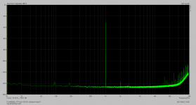
symmetrical input, 2W @ 4Ohm load
for the measuments shown i changed the input of the circuit to a symmetrical connection by using a standard cable for telephone installation (type: shielded 2x2x0,6mm in starquad configuration) and changed the load to 4Ohm. The rest of the connections are left unchanged.
Attachment 1:
symmetrical input, no signal applied. clear to see that the power supply artefakte are lower than before, but not the "distortion" at 50Hz - i have actually no idea where this comes from, as no 50Hz "source" is nearby and the first rectifier artefakte is to be expected at 100Hz...
Attachment 2:
symmetrical input, testtone 1kHz
Attachment 3:
symmetrical input, dual testtone 19kHz and 20kHz (1:1)
Attachment 4:
symmetrical input, multitone testsignal
conclusion so far:
symmetrical connection is the way to go, it is clear to see that the signal arriving the circuit is much cleaner. looks like the single ended cable works as an antenna, even when the input pins are shorted.
Attachments
Attachment 1:
symmetrical input, no signal applied. clear to see that the power supply artefakte are lower than before, but not the "distortion" at 50Hz - i have actually no idea where this comes from, as no 50Hz "source" is nearby and the first rectifier artefakte is to be expected at 100Hz...
With 50 Hz mains, you're surrounded by 50 Hz sources that will couple inductively into your circuit if you let them. That's likely also why you see the other mains-related artifacts. I'd look for ground loops and minimize their loop areas.
You can also try a faraday cage. Ideally a sealed and grounded metal box. I've had pretty decent luck with a "circuit burrito" (i.e., wrapping the circuit in antistatic bubble wrap and then in tinfoil connected to ground with a clip lead). Just be careful you don't short stuff out or allow stuff to overheat in the burrito.
-100 dBc THD is not bad. That may be the limit of your instrumentation. It certainly indicates that the error correction isn't fundamentally broken.
What's going on at 20 kHz in the latest plots?
Tom
Last edited:
I do not know if it is possible to get rid of the TDA´s fingerprint . Probably it is due to the internal biasing circuitry of the chip . It is not a complementary circuit after all . But there is one thing one can try to check this out , by configuring the device as a slave and introducing a clean already amplified signal into pin 11 . If when doing that the same k2 and k3 distortion appears in the output it is introduced in the output-stage with its biasing and protection circuitry and so probably impossible to get rid of. if not then there are other possibilities as then it comes from either the inputs , the vas or power-supply somehow ???
I would do it myself if I had the equipment to measure very low distortion , which unfortunately I do not.
I would do it myself if I had the equipment to measure very low distortion , which unfortunately I do not.
Last edited:
A faradays cage is a real good idea, because i had an eye on building NO groundloops - the "circuit burrito" described looks as an easy way to get a real cheap faradays cage, thank you Tom.
I did some work to find out what is going on at 20kHz as i have seen this "distortion" too. I am almost sure i found the origin of it - on the oscilloscope i can see a real small periodic signal as soon as the connection to the computer starts to work, its frequency is an integer multiple (6x) of 20kHz...so it has to be some kind of aliasing (not sure if this is the right word, but i hope it is clear what i meant to say). This periodic signal shows up on both soundcards i have acces to (one firewire connected, the other one USB connected, both cards terratec)
I dont know the exact limit of my instrumentation, but looking at the soundcards selftest (shown a few posts ago) you could be right that it is close to it, Tom.
The TDAs "fingerprint" is so far down in level that i dont want to make any effort to get rid of it, Mike, thanks for your ideas anyway.
while waiting for the components to arrive i did a quick test of my variation of the my_ref-circuit. The step-response test tells me it is working stable and the bandwidth (refering to my NFB circuit) is almost doubled (1W@8 Ohm), but shows a 15% peak in amplitude in the 400kHz region....
hello guys,
Has anyone seen that website - Low Distortion Composite Amplifiers LM1875 TDA7293 TDA7294
There is a lot of information about building super low distortion amplifiers based on TDA7293.
Has anyone seen that website - Low Distortion Composite Amplifiers LM1875 TDA7293 TDA7294
There is a lot of information about building super low distortion amplifiers based on TDA7293.
WLA , yes , I for one have read and studied it and the circuit diagram since you mentioned it in another thread too . I think that what is being done here , especially by bebo65 (and Tom´s considerable input as well) is superior to whats on that page . If you have not done it yet I would suggest you read the whole thread. But of course all info is wellcome so thanks .
Hello Bepo , any news concerning the myref angle ? I am digging for more info and ideas constantly and have just received 10 TDA7293 so will start experimenting with them now that I can do it the things are kind of hard to come by these days I am even considering buying a few Ebay-boards then mount a TDA on them and start modifying , so just use them as an experimental starting point
And forgive me for repeating this but I really want to figure out if the slew-rate of the TDA´s output stage is a lot better than that of the rest of the chip - since it is Mosfet that might well be the case , so we could quite possibly get a much better upper frequency-limit /less phase-shift using a discreete VAS . Greetings Michael
Hello Bepo , any news concerning the myref angle ? I am digging for more info and ideas constantly and have just received 10 TDA7293 so will start experimenting with them now that I can do it
the things are kind of hard to come by these days I am even considering buying a few Ebay-boards then mount a TDA on them and start modifying , so just use them as an experimental starting pointAnd forgive me for repeating this but I really want to figure out if the slew-rate of the TDA´s output stage is a lot better than that of the rest of the chip - since it is Mosfet that might well be the case , so we could quite possibly get a much better upper frequency-limit /less phase-shift using a discreete VAS . Greetings Michael
Last edited:
Hi Mike, good to hear from you.
I'm about to build an amplifier with TDA7293 and trying to find something really descent. According to the THD plots in the website mentioned above the design there looks really good. The type of the op amp used there is what I'd like to know. Any suggestions?
BTW what's the THD figure of the design discussed here?
Thanks
Hi WLA - its hard to recommend an op-amp as opinions about them there are many and very divided. The best you can do is note down the denominations of the various op-amps mentioned in this and other threads , then type them into the search in the whole forum and see what you come up with . Or simply use the one recommended by bepo as he is , to the best of my knowledge , the main "motor" in this thread
You will find that some people prefer using an OPA , others an LM , and so on as apart from technical specs they seem to have a different "musicality" which to my understanding is due to different internal structure and specifications , so up to a certain point it is a matter of taste.
Personally I´d go with the LM4562 or if you are willing to spend a little more the LM49720 but be advised that both seem to be identical chip inside them. The LM4562 is an 8pin DIL package so can be put into a socket to be interchangeable without soldering which is one reason I prefer it.
- Home
- Amplifiers
- Chip Amps
- TDA 7293 -- done right ?