Having completed my PAM8320 class-D project, I wanted to try a class-AB amp next, and decided on the LM3886. I know there are plenty of boards already out there, but I enjoy the process of drawing the schematic and laying out the PCB, and feel I can learn a lot more about how these things work while I do it.
I was following this post, that goes into some detail about how to choose the supporting components, but have also read a few of the threads on this forum, in particular those relating to the Neurochrome LM3886DR (having never considered it before, it just occurred to me that Tom Christiansen could be a fellow Canadian William Gibson fan, the company name being a mashup of Neuromancer and Burning Chrome... I digress!), and the open source PCBs. I also read through Tom's "Taming the LM3886 Chip Amplifier" and have attempted to apply what I've learned to my design. However as a relative newbie to electronics, let alone analogue electronics, I have struggled a bit to understand some of what's being said!
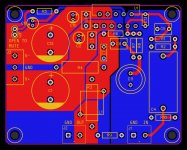
I'd be grateful for any constructive feedback on my schematic & PCB layout, including component choice. It's a first-pass so I imagine there will be issues a plenty.
I'm a tad confused how to keep the grounds separate, but join them in the particular order suggested in the article. The Circuit Basics post I mentioned above keeps everything separate and joins the various grounds at the power supply, but this is advised against elsewhere. He also suggests that capacitor Cc causes oscillation if connected between the inverting and non-inverting inputs, and advises to go directly to ground - again something the other implementations I've studied have eschewed.
I've also noticed that some implementations use a resistor before the input coupling cap, which is 10x the value of the resistor after the cap. I've not included that at the moment, because I'm not sure what it does, but could easily add it if necessary.
Thanks, Christian
I was following this post, that goes into some detail about how to choose the supporting components, but have also read a few of the threads on this forum, in particular those relating to the Neurochrome LM3886DR (having never considered it before, it just occurred to me that Tom Christiansen could be a fellow Canadian William Gibson fan, the company name being a mashup of Neuromancer and Burning Chrome... I digress!), and the open source PCBs. I also read through Tom's "Taming the LM3886 Chip Amplifier" and have attempted to apply what I've learned to my design. However as a relative newbie to electronics, let alone analogue electronics, I have struggled a bit to understand some of what's being said!
I'd be grateful for any constructive feedback on my schematic & PCB layout, including component choice. It's a first-pass so I imagine there will be issues a plenty.
I'm a tad confused how to keep the grounds separate, but join them in the particular order suggested in the article. The Circuit Basics post I mentioned above keeps everything separate and joins the various grounds at the power supply, but this is advised against elsewhere. He also suggests that capacitor Cc causes oscillation if connected between the inverting and non-inverting inputs, and advises to go directly to ground - again something the other implementations I've studied have eschewed.
I've also noticed that some implementations use a resistor before the input coupling cap, which is 10x the value of the resistor after the cap. I've not included that at the moment, because I'm not sure what it does, but could easily add it if necessary.
Thanks, Christian
Attachments
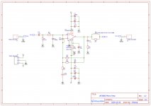
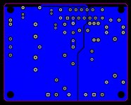
The LM3886 data sheet says that the "star layout" should be observed (look under "Layout, Ground Loops, and Stability. " You have three return grounds: one through the output ground, which in your schematic is pin 2 on the OUT+ connector, the feedback ground, which is the ground connection of C11, and the input signal ground, which is ground connections on R2 and C5.
These should be separate paths. The output ground current on J2 will return mostly to the left back to the power rails, which is good. The ground on C11 and J1 are connected by a generous wide ground plane, so it doesn't appear like there should be much of a potential drop there, especially given the low currents in the feedback loop. The only thing I can think of would be to add a hum breaker resistor of about 10 to 20 ohms between the ground on the right side of the break, which is your signal "quiet" ground and the noisy ground noisy power ground on the left side of break. Designate the grounds on J1, C11, and R2 as a separate net and then connect this to the output ground through the hum breaker resistor. Especially if you use two of these PCBs in a stereo configuration, the hum breaker can prevent cross-coupling between the two channels.
Other than that, maybe C3 is a little close to the amplifier chip so there could be problems fitting them together? You perhaps could tighten up and shrink the feedback loop surrounded by output pin, C8, R7, and V- (and of course the path on the chip between V- and the output pin). Some people think that a small capacitance NP0/C0G ceramic is not suitable, but they are smaller and don't use the high-k dielectrics that cause problems with microphonics. It will probably work fine though.
I think the idea of having the large capacitance before the coupling cap in the input is so that the DC voltage at the input is not floating and is nominally pulled to ground weakly. If, for example, the output of the preamp was similarly floating, then the input could float out of the voltage range of the coupling capacitors. I don't think its absolutely necessary.
The data sheet and Bob Cordell's LM3886 versions (which seems to mostly follow the datasheet) use the capacitor between V+ and V-, and it is recommended in the datasheet to suppress possible oscillations from coupling from output to input. So I include it.
Hi, thanks very much for your feedback. Very useful and interesting.
I *think* I've covered all your points in the latest version:
- Added a hum breaker resistor (R9) between the now input/feedback ground plane, and the left-side output/power ground
- Ground plane split changed as suggested by 00940
- Moved C3 to give the IC a bit more breathing space
- Tightened up the feedback loops (although I read somewhere that having the feedback resistor R6 too close to the IC leads was not in fact the best thing?)
I also added the resistor pre-coupling cap (R10) because there's nothing to lose by having the footprint there.
A question about the feedback capacitor C11 - what value and voltage rating should it be? I'm guessing the voltage cannot go above the peak output voltage of the amp right? So I'll be powering the amp using around +/-30v max give or take, basically rectified 18-0-18vAC, and if my calculations are correct this means the peak output voltage will be around 22 volts. So will 25v bipolar caps do, or should I plump for 35 or even 50 volt caps? Given the input components, is 100uF a good value, or should it be higher, e.g. 220uF? Just considering the size of the cap and its lead pitch for the board.
Thanks, Christian
Attachments
take a look here: A Complete Guide to Design and Build a Hi-Fi LM3886 Amplifier - Circuit Basics,
I think 25v for C11 is good enough .
I think 25v for C11 is good enough .
Feedback Resistor
Thanks.
Regarding the feedback resistor placement - can anyone point me in the direction of the post or article where Tom Christiansen goes into detail about why it's best to route the trace from the Thiele network input?
In his "Taming the LM3886 - Stability" article, Tom says that the good layout is where the resistor practically bridges pins 3 and 9, however given what he writes here, and indeed in the LM3886DR & Open Source layouts, I assume this is only best when there's no Thiele network. I was certain I'd seen somewhere a post with measurements or simulation results that explained why this was the preferred layout, but there are so many long threads on this chip-amp that I can't seem to find it!
Cheers, Christian
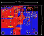
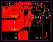
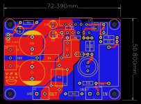
Here's the latest version of the board layout. As you can see it's a bit smaller than before, with a few things tightened up.
I got the idea to use 0805 SMD parts for the 4.7uF decoupling caps instead of the leaded ceramics. They can be hidden away on the bottom side of the board, and are practically sat on the power pins of the LM3886 (at least on one of the +V pins anyway). This also allows the 22uF electrolytics to get closer to the chip. Hopefully this will have a positive effect.
Christian
Attachments
Acceptable Gain Resistor Values
When setting the gain, what are reasonable ranges for the feedback resistor, as in min and max? I guess the standard is to go with a 20kOhm for Rf1, with a 1k for Ri, giving a gain of 21 (26.44dB).
Following the advice given in this article I should attempt to balance the input bias current of the amp with a resistor that is as close to Rf1 - Rb, which is the series resistor at the non-inverting input. So if Rb is also 1k then Rin should be around 19k.
Rin, combined with the input coupling cap sets the -3dB cutoff of the low-end, and this in turn affects the choice of capacitor Ci.
What are the advantages & disadvantages of increasing the resistor values to say Ri = 1740 Ohms, Rf1 = 33kOhms? More noise? Is it better to go lower, even if doing so will roll-off the low end quicker (assuming Cin is not changed)?
Thanks, and please forgive the newbie questions!
In practical terms, if you are moderate, say keeping within 0.5X to 2X of the suggested values, no big deal.
Without knowing or analyzing the internal circuit, I guess the designer has chosen voltage divider values (because the NFB loop is exactly that) passing, say, 10X the current needed by internal active components, so as to absorb and minimize production variations.
Why?
No hard rules for that, but it´s common practice since gain stages were made oit of a humble single transistor and had to be biased.
Same (or very similar) thing.
I would not go trigger happy and use, say, 1M:100k NFB values for example, I guess using such values would cause huge DC offset simply because of input base biasing would drop a lot through 1M
That article is good but has some excessive/misleading points. This section isn't very good at explaining things. See this article for a more correct explanation (short version, we're balancing impedances, not currents). Slightly mismatched input impedances will not increase noise in a significant fashion. It will however somewhat influence the output offset voltage. In practice, it won't be a big problem as long as you don't go crazy.
Another point: don't sweat too much over the corner frequency set by the input cap/input resistor. 1.5hz seems a tad excessive to me. Keep it under 10hz and that's fine. The lm3886 really isn't an amp to pair with a subwoofer going down to 20hz flat anyway. The point about the corner frequency set by the feedback cap is very valid though. You want it a few octaves below the frequency set by the input cap.
Another point: don't sweat too much over the corner frequency set by the input cap/input resistor. 1.5hz seems a tad excessive to me. Keep it under 10hz and that's fine. The lm3886 really isn't an amp to pair with a subwoofer going down to 20hz flat anyway. The point about the corner frequency set by the feedback cap is very valid though. You want it a few octaves below the frequency set by the input cap.
I wouldn't worry about balancing the impedances 'seen' by the two inputs of the LM3886. You'll get slightly lower offset voltage, but probably not meaningfully so. Just ensure that the circuit has a DC gain of 1 V/V (so include a capacitor in series with the resistor to ground in the feedback network). That'll give you about ±2 mV nominal offset and ±10 mV worst case.
The ~2 Hz pole is commonly chosen as it's "significantly lower" than 20 Hz, which is the lowest frequency we tend to care about. By being significantly lower, it has negligible impact on the amplitude and phase response of the amp within the audio band.
Tom
The ~2 Hz pole is commonly chosen as it's "significantly lower" than 20 Hz, which is the lowest frequency we tend to care about. By being significantly lower, it has negligible impact on the amplitude and phase response of the amp within the audio band.
Tom
Hi Tom, thanks for your comments. Not sure what led me to choosing 47uF for the mute cap (possibly something daft like its physical size), but I'm grateful for the advice - these amps are like delicate ecosystems where a wrong component, or placement can throw something off elsewhere! I've changed it to a 100uF now.
Are you referring to the feedback cap Ci? I'm using a 100uF bipolar cap here.
Cheers, Christian
(so include a capacitor in series with the resistor to ground in the feedback network)
Are you referring to the feedback cap Ci? I'm using a 100uF bipolar cap here.
Cheers, Christian
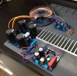
Finally after over a month in the China-Europe-UK delivery wilderness, the PCBs have arrived! Got my PSU boards (mains input, split-rail AC-DC) and the LM3886 boards on the bottom left.
Now I just need some time to sit down and solder them up. I'd hoped they'd be here by the Christmas break but Brexit and Coronavirus saw fit to put paid to that!
Now I just need some time to sit down and solder them up. I'd hoped they'd be here by the Christmas break but Brexit and Coronavirus saw fit to put paid to that!
Attachments
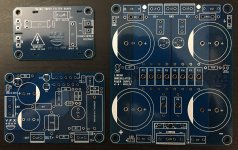
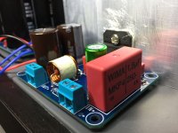
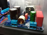
PSU and one amp board built.
PSU puts out +/-26v on the nose, using a 2x18V 160VA transformer. Powered up the amp board with no load - no magic smoke and nothing got hot (apart from the 330ohm bleed resistors on the PSU, which I under-spec'd, so they'll need to be replaced with something beefier)!
Before I connect it to a speaker I'll be running some sine wave tests into an 8-ohm resistive load, to get approximate frequency response and power output.
Attachments
Non-Listening Tests
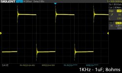
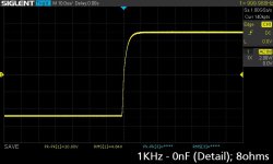
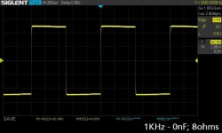
Done some preliminary testing using my signal generator. my load is 10x 82ohm 10w resistors in parallel, giving a total of 8.1ohms. I also have some flying leads to which I can plug in capacitors for oscillation tests.
The amp is set up to have 26dB gain (21Vo/Vi); Clipping occurred at over 15.85Vrms (45.02Vpk-pk) with an input voltage of 2.1V. This is with a +/-26V power supply, so I calculate just over 31Watts clean power.
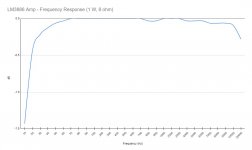
Frequency response is as expected given the input filtering. I don't have a Siglent signal generator so couldn't run an automated Bode plot with my scope, so what I have is based on Vrms readings from the scope as I dialled in different frequencies. I've seen elsewhere that these readings are usually made with 1W power, so I dialled in 0.372V, which gave 2.83Vrms from the amp at 1KHz. Given that the Vrms value varied based on the scope timebase and how many waves were on screen, there's some error to be expected in the readings, like the small dip around 800-900Hz.
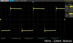
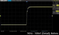
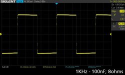
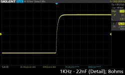
Finally I fed a square wave signal into the amp to test its stability given various capacitances on the output. I started seeing minor oscillation at 100nF (nothing with 10nF or 22nF, and I don't have any 47nF caps). The maximum I tried was 10uF, which oscillated pretty badly but recovered very quickly. I'm hoping these results show the amp is working well, and my board layout and component choices were good! Images attached.
Done some preliminary testing using my signal generator. my load is 10x 82ohm 10w resistors in parallel, giving a total of 8.1ohms. I also have some flying leads to which I can plug in capacitors for oscillation tests.
The amp is set up to have 26dB gain (21Vo/Vi); Clipping occurred at over 15.85Vrms (45.02Vpk-pk) with an input voltage of 2.1V. This is with a +/-26V power supply, so I calculate just over 31Watts clean power.
Frequency response is as expected given the input filtering. I don't have a Siglent signal generator so couldn't run an automated Bode plot with my scope, so what I have is based on Vrms readings from the scope as I dialled in different frequencies. I've seen elsewhere that these readings are usually made with 1W power, so I dialled in 0.372V, which gave 2.83Vrms from the amp at 1KHz. Given that the Vrms value varied based on the scope timebase and how many waves were on screen, there's some error to be expected in the readings, like the small dip around 800-900Hz.
Finally I fed a square wave signal into the amp to test its stability given various capacitances on the output. I started seeing minor oscillation at 100nF (nothing with 10nF or 22nF, and I don't have any 47nF caps). The maximum I tried was 10uF, which oscillated pretty badly but recovered very quickly. I'm hoping these results show the amp is working well, and my board layout and component choices were good! Images attached.
Attachments
-
 lm3886_tr_10uf_8ohms.jpg97.4 KB · Views: 80
 -
 lm3886_tr_1uf_8ohms.jpg94.6 KB · Views: 80
 -
 lm3886_tr_470nf_8ohms.jpg93.3 KB · Views: 77
 -
 lm3886_tr_220nf_8ohms.jpg93.3 KB · Views: 76
 -
 lm3886_tr_100nf_8ohms_det.jpg92.1 KB · Views: 89
 -
 lm3886_tr_100nf_8ohms.jpg91.6 KB · Views: 78
 -
 lm3886_tr_22nf_8ohms_det.jpg91.4 KB · Views: 77
 -
 lm3886_tr_0nf_8ohms_det.jpg91 KB · Views: 74
 -
 lm3886_tr_0nf_8ohms.jpg90.7 KB · Views: 86
 -
 lm3886_frequency_response.jpg42.8 KB · Views: 275
Can anyone with more knowledge than I on the subject comment on whether the transient response results are good or not, with the given capacitances?
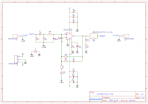
For reference, here is the schematic again with the values of components used.
For reference, here is the schematic again with the values of components used.
Attachments
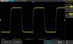
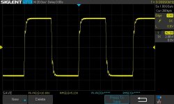
Disappointing Transient Response Tests, part 2
Having looked around on here and paid closer attention to similar tests, notably those done by tomchr when testing the XY kit and his own LM3886DR, I noticed that the transient response tests were done at 10KHz (not 1KHz as I'd previously done). I also suspected that my results weren't actually that great, and re-running the transient response tests at 10KHz proved me right.
My boards ring quite noticeably at 100nF, with 470nF and 1uF both ringing quite crazily! I tested with both my left and right channel boards, and the ringing was marginally less on the right board, on which I'd deliberately left out the 220pF Cc cap across the inputs. On-the-fly insertion of this cap using a pair of pliers made the ringing consistent with the left board, so I question whether it's valid to leave out this capacitor in future.
The results are quite disappointing, and something I'd like to understand better and fix if possible in a future revision. My Thiele Network has an inductor with 10 turns with a diameter of 10mm with 0.95mm wire, which should give the recommended 0.7uH inductance according to an online calculator, in parallel with a 10ohm resistor. I wonder if a larger (as in greater inductance) inductor might help, after all if I understand correctly it's the Thiele Network that quashes the resonance caused by a capacitive load. I'm planning on buying another set of components and making up a third board to test that theory.
I've also implemented the Zobel Network and have all the recommended stability components, except for as I said, the 220pF cap across the inputs on the second board.
Any suggestions please?
Images attached - no capacitance, 100nF, 470nF, 1uF. All tests done with an 8ohm load.
Attachments


- Status
- This old topic is closed. If you want to reopen this topic, contact a moderator using the "Report Post" button.
- Home
- Amplifiers
- Chip Amps
- Another LM3886 Amp PCB