Thanks for the beautiful work going on here, FF and others. Especially enjoyed reading FF's rationale -- about doing this instead of other useless things ")
But I'm wondering/hoping to see some testing at low frequencies -- maybe 100 Hz or so. This SPiKe stuff looks pretty darned clever to me, and being SOA-based, supply voltages, load current, and time all factor into its 'calculations'. The data PDF has a lot to say about it -- more than I'd have been able to figure out by testing.
Good stuff!
Hi Chris,
I will now try to finish the Triple in BTL version.
The modules I mention are not standard modules but modules that are adapted to our particular needs with a custom PCB.
Hi FF
Do you find something good PCB that can be used for 3p LM3886 or 3x7293?
PCB board only three parallel lm3886 3 parallel amplifier mono amplifier board lm3886 amplifier|amplifier outdoor|amplifier digital|amplifier hearing - AliExpress
2x3886
pcb board only hifi jeff rowland two parallel btl mold lm3886 2 parallel Jeff Rowland mono amplifier board lm3886 amplifier|amplifi|pcb power amplifier|amplifier used - AliExpress
Last edited:
Hi Chris, I have found boards for up to three TDA7293 or two LM3886 as I recall.
I would try such small parallel-boards for test purposes only but not if I had to make an amplifier for real use. The reasons is that none of the boards you show or I found have space for any sufficient power line decoupling when you parallel-couple high-power chip-amps with the aim to handle high currents. The boards seem only to include the very basic capacitance preventing the ICs from oscillating but no more. Next, when you parallel-couple chip-amps for high current, the PCB layout becomes an important issue.
PCB layout for 2-3 A may not require much reflection but when you exceed 10 A, the layout has to match that current. Without having studied in details the PCBs you show, I fear they are made according to usual standards but not adapted to high current use.
What I would do if I for instance had to make a triple LM3886 amplifier was to buy three small mono-boards with a good layout. Then, the current handled on one board will not exceed the current for a single IC. The three LM3886 mono-boards, I would mount on one side of a big main-board. On one side of the main-board, I would solder wire-tracks with dimensions suited for high currents such that these high current tracks are located underneath the mono-boards. On the side of the main-board opposite of the high current tracks and the mono-boards, I would arrange sufficient power line decoupling (probably some 2x20.000uF) such that the decoupling capacitors are connected to the high current tracks. Connecting each of the mono-boards to the high current tracks as well leaves an assembly that is designed to handle high currents.
It will form an amplifier block rather than a flat amplifier board but the performance will be better due to short, high current suited connections.
Thanks for the beautiful work going on here, FF and others. Especially enjoyed reading FF's rationale -- about doing this instead of other useless things
But I'm wondering/hoping to see some testing at low frequencies -- maybe 100 Hz or so. This SPiKe stuff looks pretty darned clever to me, and being SOA-based, supply voltages, load current, and time all factor into its 'calculations'. The data PDF has a lot to say about it -- more than I'd have been able to figure out by testing.
Good stuff!
Hi Rick,
We are happy to hear that our activities are appreciated by others.
The 100Hz testing will be put on the stack for future action.
My impression is that TI has put a lot of effort into SPiKe and used it in several of their chip-amp designs. I am convinced that the chips are well protected but as a user I also like the influence on amplifier performance to be predictable. There I for a start had some problems and surprising curve-shapes would appear. Now it seems much better and also Turbowatch2 is putting his vast experience into the analysis.
Tom from Neurochrome talks about "taming" the LM3886. Perhaps an important part of the "taming" is understanding the influence from SPiKe.
For the high current 'rails', how about strips of 0.032" copper, maybe a cm wide, placed top-side and perpendicular to the PCB. Then use tinned #20-or-so buss wire in a loop over the top of the strip, behaving as through-hole component legs to serve up the power, gnd, or output connections as needed.
Most hobby shops/stores have a 'K & R Metals' display/end cap -- brass, aluminum tubings in various shapes, plus some flat stock. I've found the heavy copper darned handy for a number of things electronic. A nice 4 x 10" chunk (the standard packaged size, IIRC) will last through several projects.
Just a thought ..
Cheers
Last edited:
Hi Rick,
I was thinking along the similar lines…the idea has already been used in many amplifiers, from the initial Rotel amp models to the high-end, high power professional Yamaha amp models. The idea greatly helps distribute the power from the input (rectifier, main filter capacitors) through the output transistors to the speaker output, and at the same time, if Vcc/Vee and power ground return are in close proximity high current ac loop will be minimal, and at the same time simplifies the pcb.
I was thinking along the similar lines…the idea has already been used in many amplifiers, from the initial Rotel amp models to the high-end, high power professional Yamaha amp models. The idea greatly helps distribute the power from the input (rectifier, main filter capacitors) through the output transistors to the speaker output, and at the same time, if Vcc/Vee and power ground return are in close proximity high current ac loop will be minimal, and at the same time simplifies the pcb.
Last edited:
I have ordered some of these a while ago. About 6$ each. Not the best design you can think of, but IMO much better than the green ones.
I use such kind of silver coated copper wire, as pictured at the top, to improve the low frequency reproduction. Even these small distances at the PCB are audible with high current.
PS the values of the parts are reasonable, only the 47pF capacitors should be smaller, about 8pF.
Note that you do not need to reinforce the ground on the PCB if you use two of these bridged.
24V AC should give a very tough amp, able to drive any speaker. You can combine one bridge with two cheap 250 W 36V SMPS, this would make it really a bargain. In tests of the different JRD amps, the ones with SMPS where found to sound even better. In any case, a SMPS is no disadvantage. In such a case the capacitors on the board, if high quality, should be enough. Just place some 2uF Wima or the like at the underside, directly at the chips pins.
Attachments
Last edited:
Hi Turbo
WOW-this board looks promising. i cannot find it at aliexpress.
i just found a similar version with through hole components:
one piece LM3886 3 series single channel postgrade power amplifier PCB empty board|Amplifier| | - AliExpress
chris
WOW-this board looks promising. i cannot find it at aliexpress.
i just found a similar version with through hole components:
one piece LM3886 3 series single channel postgrade power amplifier PCB empty board|Amplifier| | - AliExpress
chris
That looks a lot like the boards shine7.com used to build the 300W BTL monoblocks that you linked in post #68 ..
.. is that them? Do you happen to know if they're still available? Just curious.
Hi aparatus, Yah -- was thinkin' I'd seen that somewhere in commercial gear, just couldn't remember where -- didn't mean to sound like I was taking credit for the idea! Rotel and Yamaha, huh? Alrighty, thanks.
.. is that them?
Do you happen to know if they're still available? Just curious.Hi aparatus, Yah -- was thinkin' I'd seen that somewhere in commercial gear, just couldn't remember where -- didn't mean to sound like I was taking credit for the idea!
Rotel and Yamaha, huh? Alrighty, thanks.The through hole looks fine, I would prefer it, as I like old style components and have ton´s of them. If you have to buy parts, the SMD is probably better. You get 0.1% resistors in SMD, which is a very important. The better you match components, the lower you can make the in line resistor at the output. .1-.2 Ohm/ 3 Watt should do. Only with real LM3886, off course!
If anyone wants to build such an amp, there are some things to think off. For example the output should get a L-R which can be at the output posts. Read at shine7.com and "taming the LM3886" before you start a build.
PS SMD board
1pcs lm3886 x3 Parallel 150w HIFI Pure DC Mono Endstufe Bare Board | eBay
Hi Turbowatch2,
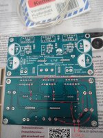
I don't think this pcb is made properly ... in the picture I have drawn where the positive going signal from + Vcc connector goes -> via pcb plane/trace -> Amp(s) -> balancing resistor(s) -> output trace(s) -> + speaker connector -> load -> then back via -> ground connector -> ground plane/trace -> main capacitor(s) - and finally again at +Vcc plane/trace, so the process is repeated again as specified above. There is no local decopling near each amp, so the (large) loop is the same for all frequencies that the amp can handle, from pure DC to xy Mhz. The same thing happens for the negative going signal also just on the other side of the pcb.
I don't think this pcb is made properly ... in the picture I have drawn where the positive going signal from + Vcc connector goes -> via pcb plane/trace -> Amp(s) -> balancing resistor(s) -> output trace(s) -> + speaker connector -> load -> then back via -> ground connector -> ground plane/trace -> main capacitor(s) - and finally again at +Vcc plane/trace, so the process is repeated again as specified above. There is no local decopling near each amp, so the (large) loop is the same for all frequencies that the amp can handle, from pure DC to xy Mhz. The same thing happens for the negative going signal also just on the other side of the pcb.
Hi Turbowatch2,
I don't think this pcb is made properly ... in the picture I have drawn where the positive going signal from + Vcc connector goes -> via pcb plane/trace -> Amp(s) -> balancing resistor(s) -> output trace(s) -> + speaker connector -> load -> then back via -> ground connector -> ground plane/trace -> main capacitor(s) - and finally again at +Vcc plane/trace, so the process is repeated again as specified above. There is no local decopling near each amp, so the (large) loop is the same for all frequencies that the amp can handle, from pure DC to xy Mhz. The same thing happens for the negative going signal also just on the other side of the pcb.
Let's see if it works now...I had some problems syncing the Onedrive app.
Attachments
@aparatusonitus
This is not my design and I do not see it as the best you can do.
Anyway, it is very close to the one "shine7" used and this works well single ended and bridged.
Then, there is often a basic misunderstanding between high frequency theory and the reality of a band limited amps, cruising around 10-50.000Hz. Which is noting where you get exited about high frequency electromagnetic stuff.
As we say in German: " Leave the church in the village".
The chip is getting tired at 100 kHz.
Maybe have a look into your cell phone, there you go with .8-5 MHz all day long.
If you tune your Lada, not all rules from Formula 1 may fit.
I do not understand the problem you see, any amp has to run in such a loop.
Maybe you can explain the solution you see for the problem?
Please do not forget, there are film capacitors that have to be soldered directly at the chips legs from the underside of the PCB. Making the way as short as can be. Then, as I mentioned, some extra copper over the traces will be beneficial.
People see all kind of problems with these chips that do not exist if you buy a real one, no China clone. I bet the Chinese fakers sell a lot more fake 3886 than TI real LM3886.
If you trust these chips, you ask for trouble.
The real one is quite tolerant to parts value, component quality and layout. This is most important for OEM producers and a cause while it is still around.
The Boucherot cell is external, usually at the speaker posts at the back of the case.
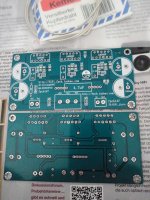
The board is much smaller than it looks, it is just 6 cm x 12 cm. You get two on a 25 cm / 10" heat sink. So parts are close together.
Last, in a bridge amp the current flow is from one amps + to the other ones inverted +. So ground is not directly involved.
Please, don´t get me wrong, share your ideas, that is why we communicate here!
Thank you!
PS my single chip, low cost China 3886 build has an output offset of .5 mV. With input closed, output open (same with 4 Ohm load). Without any servo or trimmer. I have seen other builds measuring 16 mV after trimming. Something to think of. As my projects go slow, I can not share more about these 3x boards. I will sure buy my chips at Mouser, DigiKey or RS and select them for groups of similar offset.
This is not my design and I do not see it as the best you can do.
Anyway, it is very close to the one "shine7" used and this works well single ended and bridged.
Then, there is often a basic misunderstanding between high frequency theory and the reality of a band limited amps, cruising around 10-50.000Hz. Which is noting where you get exited about high frequency electromagnetic stuff.
As we say in German: " Leave the church in the village".
The chip is getting tired at 100 kHz.
Maybe have a look into your cell phone, there you go with .8-5 MHz all day long.
If you tune your Lada, not all rules from Formula 1 may fit.
I do not understand the problem you see, any amp has to run in such a loop.
Maybe you can explain the solution you see for the problem?
Please do not forget, there are film capacitors that have to be soldered directly at the chips legs from the underside of the PCB. Making the way as short as can be. Then, as I mentioned, some extra copper over the traces will be beneficial.
People see all kind of problems with these chips that do not exist if you buy a real one, no China clone. I bet the Chinese fakers sell a lot more fake 3886 than TI real LM3886.
If you trust these chips, you ask for trouble.
The real one is quite tolerant to parts value, component quality and layout. This is most important for OEM producers and a cause while it is still around.
The Boucherot cell is external, usually at the speaker posts at the back of the case.
The board is much smaller than it looks, it is just 6 cm x 12 cm. You get two on a 25 cm / 10" heat sink. So parts are close together.
Last, in a bridge amp the current flow is from one amps + to the other ones inverted +. So ground is not directly involved.
Please, don´t get me wrong, share your ideas, that is why we communicate here!
Thank you!
PS my single chip, low cost China 3886 build has an output offset of .5 mV. With input closed, output open (same with 4 Ohm load). Without any servo or trimmer. I have seen other builds measuring 16 mV after trimming. Something to think of. As my projects go slow, I can not share more about these 3x boards. I will sure buy my chips at Mouser, DigiKey or RS and select them for groups of similar offset.
Last edited:
Maybe you can explain the solution you see for the problem?
The solution is not to use that pcb...you will never achieve datasheet performance using it. Due to the large, high ac current loop inside which there are very sensitive signal nodes, various spurious signals will be generated and superimposed to an input signal that is yet to be amplified, and depending on whether such signals nodes are inside or outside the negative feedback loop, the same will be corrected or not.
You will be better served if you make the p2p variant yourself, using knowledge from neurochrome sites, using low impedance, close coupled traces for all input and output high ac current signals, also taking into account power supply decoupling and how and where to connect signal gnd to amplifier power gnd...exactly as Tom Christiansen explained.
See, I´m a technician, no religious fanatic with HIFI.
Ok, you have your knowledge from neurochrome. Tom C. is a gifted engineer and a great sales man. I´m happy that such wonderful creations like his exist, even if they may not be for anyone.
For people with lower expectations, even a simple LM3886 like TI/ National have it in their datasheets will work, for others, like you maybe, not. Even if you only guess that they are worse, not know. Did I mention religion?
Poor people like me have only an oscilloscope capable 20 MHz, so what is even further up there is out of my view. But for others this may be the region important for ultimate sound quality.
I have been building kit amps for more than 45 years now. Small details can make huge sound differences and some huge construction details can badly disappoint in an objective A-B test. Which is the final criteria for me.
For example, I bet my house, car and two daughters, that you will not hear the difference of an .2mV output offset and 50mV.
That does not mean you may not feel better with .2mV!
The through hole looks fine, I would prefer it, as I like old style components and have ton´s of them. If you have to buy parts, the SMD is probably better. You get 0.1% resistors in SMD, which is a very important. The better you match components, the lower you can make the in line resistor at the output. .1-.2 Ohm/ 3 Watt should do. Only with real LM3886, off course!
If anyone wants to build such an amp, there are some things to think off. For example the output should get a L-R which can be at the output posts. Read at shine7.com and "taming the LM3886" before you start a build.
PS SMD board
1pcs lm3886 x3 Parallel 150w HIFI Pure DC Mono Endstufe Bare Board | eBay
Thanks Turbo.
I guess for non composite amp - an amp with "just" 3x parallel would be sufficient for me...
chris
See, I´m a technician, no religious fanatic with HIFI.
As such, I perceived you too...otherwise I wouldn't bother.
Ok, you have your knowledge from neurochrome.
Your assumption is wrong...I can say, without false modesty, that I have mostly learned the important bits and piaces from the real giant (it is a real big loss for all of us that he is no longer able/want to participate in the discussion here and elsewhere as much as I would like)...his forum nick is ilimzn, here and elsewhere. As luck would have it, he was also from Croatia, so an entire generation from Croatia had the opportunity to study online basic and advanced electronics for over a decade.
To the vast majority of us, he clearly explained and practically showed why /how the ac currents in the amplifiers/psu flow...neurochrome was able to implement this from a to z, so I mentioned him as a good reference.
That's all, no religion involved, no audiofoolery...purely technical.
For people with lower expectations, even a simple LM3886 like TI/National have it in their datasheets will work, for others, like you maybe, not.
Believe it or not, a correctly implemented schematic from NS datasheets works for me to.
For example, I bet my house, car and two daughters, that you will not hear the difference of an .2mV output offset and 50mV.
That does not mean you may not feel better with .2mV!
It's not clear to me why you even mention the DC offset output every once in a while
...we're not talking precision opamps here...and to answer the question, I could not care less for a DC offset within reasonable limits for an output amplifier.I think technically we are not so far apart as it might seem, it is just another view with weight put on different edges.
What you say is all very true, if you build a discreet amp from scratch, but with such a chip, the advantage is that 90% of the critical stuff done inside. On the outside there are just a few variable parts and such of high volume. If someone starts to tell me about nH inductance and shows me advantages in the MHz region of some combined parts, I scratch my head and ask if this is relevant for me and the LM3886 amp that does not even operate at more than 100kHz. Also, why do I have to design my a*s off, just to get distortion from .001 to .0005 %. All these improvements are real, but how do they turn out to the listening audience?
The answer is easy: For some it matters, for others not. I´m more the "not" type of guy. I´m happy that out there are talented engineers that push limits, but some may only matter as interesting data. I don´t believe in overestimating single parameters, but count on the combination of the whole package.
If you have read my previous posts carefully, you will know that I questioned this board from the first moment it was mentioned and advised not to use it as is. There are quite some things to be improved and modified. For you it may be the best way to design your own, new, better board, for others, modifying something worth 20$ is a better way. In my country even the PCB material costs more than the Chinese board. I have etched my first own design PCB when I was not even 14 years old. By the way, was a STK Hybrid amp that worked more than 10 years, until I disassembled it. So I know a bit about this stuff.
From what I see in this specific board is a nice, simple opportunity to build something interesting. If it turns out to sound bad, what I really don´t expect, even that does not matter, as it is "hobby". You do not loose anything, as you do it for recreation, not profit. Worst case, I will take the more expensive parts for another project and throw, maybe 40$, in the bin.
If you want to add something constructive to this thread, fine, if you only want to troll, no problem, go on, there is an ignore button.
Tom´s neurochrome amps are not the theme here, he has enough pages filled with his premium stuff. Maybe in half a year I will buy a few of his boards, but now I want to play...
- Status
- This old topic is closed. If you want to reopen this topic, contact a moderator using the "Report Post" button.
- Home
- Amplifiers
- Chip Amps
- Chip-amps suited as power stage in a composite amplifier, LM1875/TDA2050 excluded.