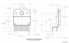
Reading a datasheet for LM3886 integrated amplifier, I found the pins span at most 2.7cm, but when I received the actual chip, this was around 2cm. Since, I have the PCB readily etched, I would like to know what other did in circumstances like these. One drastic solution is to create another PCB, but I am trying to avoid having to do that. Another one, seems to be, creating a chip footprint adapter, but this requires further etching.
I would like to avoid using wires to connect the amplifier ICs to the PCB. This is awful to look at and can cause short circuited connections.
What do you think?
I would like to avoid using wires to connect the amplifier ICs to the PCB. This is awful to look at and can cause short circuited connections.
What do you think?
In my experience parts ordering is next-day delivery, pcbs are 2 or 3 weeks. Order the parts before placing the pcb order, print out the pcb lifesize and check all the footprints _before_ placing the pcb order. Hey, you can even breadboard the circuit or parts of it to check it works too ")
Also ... It seems like spinning up an "adapter" PCB will create more issues (and is still a bodge)I'm sure a little re-shaping of the pins would solve the issue.
They are, after all, flexible enough.
I'm sure a little re-shaping of the pins would solve the issue.
They are, after all, flexible enough.
I would go for that too.
I have done that before.
I messed up many years ago with an IC footprint.
The pins were part of a millimetre apart so I found nearest imperial measurement and used that.
Because it was out slightly the error accumulated until at the last pin the pad was half a pad out.
After that I always printed out the footprint and put the ic on it to check.
If it didn't fit I adjusted accordingly.
Last edited:
Sadly, blank PCBs are now very very poor quality! Even the copper laminate's colour looks too yellowish. I repeated the PCB production ritual several times, but every time I got very poor results. The PCB metal, for I have no idea what it is made of, looks extremely thin online.
This laterally inverted PCB with too big footprints for this chips can be used provided I create an adaptor PCB. The latter has to also provide for chip lateral inversion. I designed one already but I omitted pins marked as NC.
This laterally inverted PCB with too big footprints for this chips can be used provided I create an adaptor PCB. The latter has to also provide for chip lateral inversion. I designed one already but I omitted pins marked as NC.
In my experience parts ordering is next-day delivery, pcbs are 2 or 3 weeks. Order the parts before placing the pcb order, print out the pcb lifesize and check all the footprints _before_ placing the pcb order.
Yep! I do that on all boards that use a new footprint. I usually print out the PCB top layer 1:1 and put the paper on a piece of ESD foam. I then align the part with the footprint and push the pins through the paper and into the foam. I also double-check the dimensions of the pins with the hole dimensions in the layout software.
The pins were part of a millimetre apart so I found nearest imperial measurement and used that.
Because it was out slightly the error accumulated until at the last pin the pad was half a pad out.
Oy... Yeah. I maintain a library of imperial/SAE footprints and one of metric footprints. The metric one has its units set to metric, so the layout tool handles all the necessary conversions.
I also discovered the PCB layout is laterally inverted.
Oops. Yeah. You have to be careful with "top view" vs "bottom view" when reading data sheets.
For a one-off prototype, bending the pins to make it match the footprint works well enough. An inverted board would make me grumble, kick myself, and go etch another board.
Tom
Sadly, blank PCBs are now very very poor quality! Even the copper laminate's colour looks too yellowish.
Try JLPCB. I use them for all my projects and the quality is very good and one of the cheapest out there. I can have PCB's within 2 weeks.
Seconded (but it's JLBPCB).Try JLPCB. I use them for all my projects and the quality is very good and one of the cheapest out there. I can have PCB's within 2 weeks.
I always printed out the footprint and put the ic on it to check. If it didn't fit I adjusted accordingly.
Many printers won't print exactly to scale without tweaking, so always add something to the printout
for which you know the exact dimensions, to verify.
Seconded (but it's JLBPCB).
We both screwed it up! 😆
PCB Prototype & PCB Fabrication Manufacturer - JLCPCB
I also discovered the PCB layout is laterally inverted....
Put the chip on the back side.
[emoji2357][emoji2357][emoji2357]
You need to replace your gramophone needle or your laser in your CD player.ubergeeknz said:What to do about mismatched IC footprints? x3
The external circuitry for the LM3886 chip amplifier consists essentially of:
- the negative feedback potential divider plus series capacitor to ground
- the input filter; a potential divider plus input DC isolating capacitor
- the output filters; an LR filter in series with the load and an RC filter in parallel with the load but connected before the LR filter.
- a resistor pulling pin 8 (mute) down to rail -ve. Here, the current out of this pin must be >= 0.5mA, otherwise, the chip stays in mute mode. Mute can be enhanced by exploiting the output characteristic of a BJT. Essentially, the sub-circuit is a current source whose driving bias is increased as the circuit is powered on.
I am manually 'designing' a PCB layout to include these additional circuit elements. I have already another chip amplifier that I built 15 years ago based on the chip TDA8563AQ. The original chip was TDA8560Q.
JLCPCB
PCB Prototype & PCB Fabrication Manufacturer - JLCPCB
Solid manufacturer for prototypes
I've got boxes of boards that are outdated and such
Endless improvements
PCB Prototype & PCB Fabrication Manufacturer - JLCPCB
Solid manufacturer for prototypes
I've got boxes of boards that are outdated and such
Endless improvements
Last edited:
Since locally available blank PCBs are very very low quality, I had to be contented with the inverted PCB, which has IC footprints almost twice as big as needed. To work around the huge footprint real estate and the pin lateral inversion, I designed two small PCBs to hold the chips and to flip the connections. Many parts of the circuit are now assembled. The chips, the large power supply decoupling capacitors, the negative feedback chains and the input filters are installed except the input capacitors. This allowed me to do the first testing of the circuit with a weak power supply that can provide a few hundreds of milliamps. The rail voltages remained at 12V and the DC offset voltages were around 1.5mV and 3.5mV. This means, the inversion was successful and the chips are working.
The next thing is to provide for amplifier switch on delay using mute, pin 8. If anyone can provide a simple one transistor circuit for that, please post. Pin 8 requires a current >= 0.5mA to flow out towards the negative rail for mute to be disabled.
The next thing is to provide for amplifier switch on delay using mute, pin 8. If anyone can provide a simple one transistor circuit for that, please post. Pin 8 requires a current >= 0.5mA to flow out towards the negative rail for mute to be disabled.
- Status
- This old topic is closed. If you want to reopen this topic, contact a moderator using the "Report Post" button.
- Home
- Amplifiers
- Chip Amps
- What to do about mismatched IC footprints?